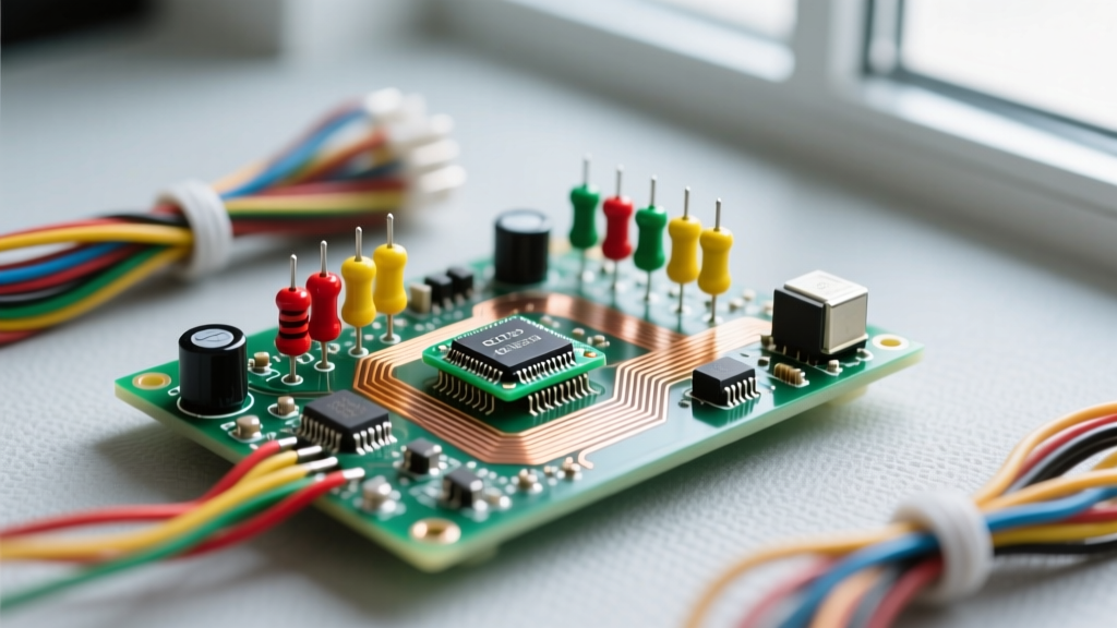
Translating a working breadboard circuit into a manufactured Printed Circuit Board (PCB) is where many hobbyist projects fail. Understanding PCB basics is not just about knowing what a substrate is; it is about managing current density, parasitic reactance, and thermal limits. This guide skips the abstract theory and gives you the exact trace widths, soldering profiles, and testing protocols needed to get a functional board on the first spin.
The Core PCB Basics: Layers, Stackups, and Material
Before routing a single trace, you must define your stackup. For 90% of maker and IoT projects, a 2-layer board is sufficient. The industry standard substrate is FR4 (Flame Retardant 4), a woven fiberglass epoxy laminate. However, not all FR4 is equal. You need to check the Tg (Glass Transition Temperature). Standard Tg130 FR4 softens at 130°C, which can cause warping during lead-free assembly or high-current operation. Always specify Tg155 or higher (like Shengyi S1000-2 or Isola 370HR) for modern prototyping.
Copper weight is measured in ounces per square foot (oz/ft²). A 1oz copper layer is approximately 35 µm (1.37 mils) thick. While 1oz is standard for signal and low-power routing, high-current paths (like motor drivers or LiPo charge circuits) often require 2oz (70 µm) copper to keep trace widths manageable and prevent the board from acting as a slow-blow fuse.
Trace Width vs. Current: The Copper Weight Matrix
The most common question in PCB layout is: what trace width does this current need? Relying on outdated IPC-2221 charts will result in overly conservative, unrouteable widths. Modern layout uses the Saturn PCB Toolkit based on the IPC-2152 standard, which accounts for board thickness and copper planes acting as heatsinks.
The table below provides required trace widths for external layers with a 10°C temperature rise over ambient. If your trace is on an internal layer, you must roughly double these widths due to the lack of convective cooling.
| Target Current (A) | 1oz Copper Width (mils) | 1oz Copper Width (mm) | 2oz Copper Width (mils) | 2oz Copper Width (mm) |
|---|---|---|---|---|
| 0.5A | 10 mil | 0.25 mm | 6 mil | 0.15 mm |
| 1.0A | 20 mil | 0.50 mm | 12 mil | 0.30 mm |
| 2.0A | 50 mil | 1.27 mm | 30 mil | 0.76 mm |
| 3.0A | 80 mil | 2.03 mm | 50 mil | 1.27 mm |
| 5.0A | 150 mil | 3.81 mm | 90 mil | 2.28 mm |
| 10.0A | 400 mil | 10.16 mm | 250 mil | 6.35 mm |
Breadboard to PCB: Mistakes That Survive the Migration
Solderless breadboards hide electrical sins. They possess parasitic capacitance (typically 2-5pF between adjacent rows) and high contact resistance (0.1Ω to 0.5Ω). When you move to a PCB, these parasitics vanish, and circuits that worked perfectly on the bench will oscillate or brownout. Here is the migration checklist to ensure these mistakes do not survive the transition:
- Missing Decoupling Capacitors: On a breadboard, the long jumper wires act as accidental LC filters, and the row capacitance smooths high-frequency noise. On a PCB, you must place a 100nF X7R ceramic capacitor within 2mm of every VCC/GND pin on every IC. No exceptions.
- Daisy-Chained Grounds: Breadboard ground rails are highly inductive. If you daisy-chain ground connections on your PCB, high-current switching (like a MOSFET driving a motor) will inject ground bounce into your microcontroller's ADC. Use a continuous copper ground plane on Layer 2.
- Floating CMOS Inputs: A floating input on a 74HC series chip might settle to a valid logic state on a breadboard due to ambient leakage. On a PCB, it will act as an antenna, oscillate at MHz frequencies, and overheat the chip. Tie all unused inputs to VCC or GND with a 10kΩ resistor.
- Ignoring Return Paths: High-frequency signals need a continuous reference plane directly beneath them. If you route a 50MHz SPI clock trace over a split in your ground plane, you create a massive loop antenna that will fail EMI testing and corrupt your data.
Workshop Safety & Soldering Specs for Assembly
Assembling your first-spin board requires precise thermal management and strict safety protocols. Soldering without defining your alloy and temperature is a fast track to lifted pads and cold joints.
Alloy and Temperature Matrix:
- Sn63/Pb37 (60/40 Eutectic Leaded): Melts at 183°C. Set your iron tip to 315°C (600°F). This is the most forgiving alloy for hand assembly, offering excellent wetting and a shiny, reliable joint. Use a no-clean or water-soluble flux core.
- SAC305 (Sn96.5/Ag3.0/Cu0.5 Lead-Free): Melts at 217°C. Set your iron tip to 350°C (660°F). Lead-free requires more thermal mass. If your iron cannot maintain 350°C under load, you will create dull, grainy cold joints. Use a high-activity tacky flux (like Amtech NC-559-V2-TF) for rework, as the factory flux core burns off too quickly at these temperatures.
First-Spin Board Testing Protocol
When your boards arrive from the fab, do not just plug them into a 5V wall adapter. A shorted via or a backwards tantalum capacitor will destroy your board and potentially your power supply. Follow this exact testing sequence for every first-spin board:
- Visual Inspection (10x Loupe): Before applying power, inspect all QFN, SOIC, and 0603 footprints under a 10x magnification loupe or a digital microscope. Look for solder bridges between adjacent pins and tombstoned passives.
- The DMM Short Check: Set a high-quality multimeter (like a Fluke 87V) to continuity or resistance mode. Probe VCC to GND. You should read an open circuit or a high resistance (>10kΩ). If you read a brief low resistance that slowly climbs, that is just decoupling capacitors charging—this is normal. If it stays below 5Ω, you have a hard short. Stop and find it.
- Staged Power-Up (Current Limited): Never use a wall wart for first power. Use a programmable bench supply (like a Rigol DP832 or Korad KA3005P). Set the voltage to your target (e.g., 5.00V) and set the current limit (OCP) to 50mA above your expected idle draw. Turn on the output.
- Thermal Sweep: If the bench supply hits the current limit and drops into Constant Current (CC) mode, you have a fault. While the board is powered in this limited state, use a thermal camera (like a FLIR ONE) or carefully use your finger to find the hot component. A reversed diode, a shorted MLCC, or a misoriented LDO will light up instantly on thermal.
Decision Tree: Picking Your Prototype Fab & Stackup
Choosing a fabrication stackup can cause analysis paralysis. Use this decision path to lock in your manufacturing specs. Do not over-engineer a simple IoT sensor, and do not under-spec a power inverter.
| Condition / Requirement | If YES, Choose This Spec | If NO, Proceed To |
|---|---|---|
| Does the circuit handle RF signals > 1GHz or controlled impedance < 50Ω? | Rogers 4350B or Isola I-Tera, 4-layer impedance controlled. | Next row. |
| Are there continuous DC traces carrying > 5 Amps? | 2oz Copper weight, minimum 1.6mm board thickness for rigidity. | Next row. |
| Is it a standard microcontroller, sensor, or low-power IoT project? | DEFAULT PICK (See Below) | N/A |
The Default Recommendation: For 95% of hobbyist, Arduino, ESP32, and Raspberry Pi HAT projects, do not waste money on exotic materials or 4-layer stackups. Order the JLCPCB Standard 2-Layer Stackup: FR4 TG155, 1.6mm thickness, 1oz copper, HASL Lead-Free finish, and 1.6mm minimum via drill. This specific combination (often listed under their standard capabilities) provides the best balance of mechanical rigidity, thermal survival during assembly, and low cost (typically under $5 for five boards), giving you a reliable baseline to iterate from.