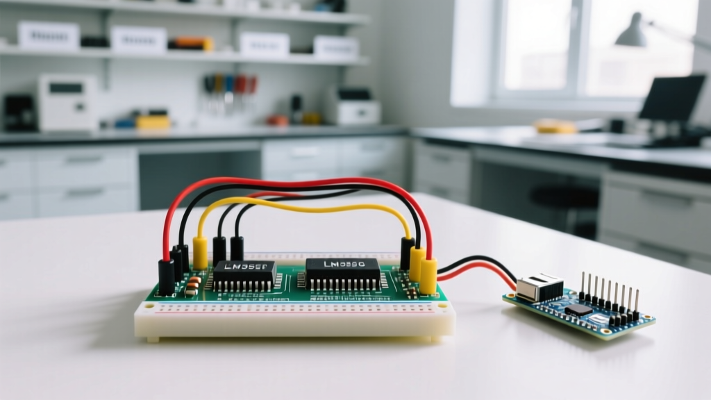

The Core Topology: Wiring an Op Amp as a Comparator
A standard comparator topology relies on five primary nodes. Unlike an amplifier circuit, there is no feedback resistor tying the output back to the inverting input to stabilize the gain. The open-loop gain of a typical op-amp is over 100,000, meaning a microvolt difference between the inputs is enough to saturate the output.
- Node 1: Non-Inverting Input ($V_{IN+}$): Typically receives the stable Reference Voltage ($V_{REF}$).
- Node 2: Inverting Input ($V_{IN-}$): Typically receives the Signal Voltage ($V_{SIG}$) you want to monitor.
- Node 3: Output ($V_{OUT}$): Swings to $V_{CC}$ (HIGH) when $V_{IN+} > V_{IN-}$, and to $GND$ (LOW) when $V_{IN+} < V_{IN-}$.
- Node 4: $V_{CC}$: Positive supply rail. Must exceed the maximum expected input voltage.
- Node 5: $GND$ / $V_{EE}$: Ground or negative supply rail.
Design Walkthrough: 12V Battery Low-Voltage Cutoff
Let’s design a real-world circuit: an alarm that triggers when a 12V lead-acid battery drops below 10.5V (indicating a deeply discharged state). We will use the ubiquitous LM358 dual op-amp, which costs roughly $0.15 in bulk and operates on a single supply.
1. Establish the Reference Voltage ($V_{REF}$)
We need a stable reference that won't sag as the battery voltage drops. A simple resistor divider tied to the dying battery is useless here. Instead, we use a 5.1V Zener diode (1N4733A) in series with a 1kΩ resistor connected to the 12V rail. This provides a rock-solid 5.1V reference to the Non-Inverting Input ($V_{IN+}$).
2. Scale the Signal Voltage ($V_{SIG}$)
The battery voltage (12V nominal) exceeds the 5.1V reference, so we must scale it down using a voltage divider at the Inverting Input ($V_{IN-}$). We want the scaled voltage to equal exactly 5.1V when the battery hits our 10.5V threshold.
Using the divider formula $V_{OUT} = V_{IN} \times (R2 / (R1 + R2))$:
Let R1 = 22kΩ and R2 = 18kΩ.
At 10.5V: $V_{SIG} = 10.5 \times (18 / 40) = 4.72V$.
At 12.0V: $V_{SIG} = 12.0 \times (18 / 40) = 5.40V$.
3. Calculate Hysteresis
To prevent the alarm from buzzing on and off if the battery rests exactly at 10.5V, we add a 4.7MΩ feedback resistor from $V_{OUT}$ to $V_{IN+}$. When the output swings HIGH (approx 10.5V on an LM358 powered by 12V), this resistor injects a tiny current into the Zener node, raising the threshold by about 120mV. The battery must now recover to ~10.65V to reset the alarm.
Behavior Matrix: Component Changes and Failure Extremes
Understanding how a circuit fails is just as important as knowing how it works. Here is what happens when elements drift, open, or short in the topology above.
| Element Changed / Failed | Resulting Circuit Behavior | System Consequence |
|---|---|---|
| Zener Diode (Shorted) | $V_{REF}$ drops to 0V. $V_{IN+}$ is always lower than $V_{IN-}$. | Output stays permanently LOW. Alarm never triggers, battery over-discharges. |
| Hysteresis Resistor $R_H$ (Open) | Positive feedback loop broken. Dead band eliminated. | Output oscillates wildly (chatter) when battery is exactly at 10.5V due to micro-noise. |
| Sense Divider R1 (Open) | $V_{SIG}$ node floats or pulls to GND via R2. $V_{IN-}$ drops to 0V. | Output immediately swings HIGH. False alarm triggers even if battery is fully charged. |
| Sense Divider R2 (Shorted) | $V_{SIG}$ pulled directly to GND. $V_{IN-}$ = 0V. | Identical to R1 open; permanent false alarm state. |
| $V_{SIG}$ exceeds $V_{CC}$ | Internal ESD diodes conduct, clamping the pin. | Excessive current flows into the $V_{CC}$ rail. Can cause latch-up or destroy the IC if not limited. |
Breadboard Testing: Step-by-Step Verification
Do not just wire it up and flip the power switch. Follow this sequence to verify the nodes safely.
- De-energize and Isolate: Ensure your bench power supply is OFF. Do not connect the actual 12V battery yet; use a bench supply set to 12V for safe testing.
- Wire the Power Rails: Connect LM358 Pin 8 to $V_{CC}$ (12V) and Pin 4 to $GND$. Place the 1N4733A Zener and 1kΩ resistor across the rails to establish the 5.1V reference.
- Verify the Reference: Turn on the power supply. Use your DMM to measure the voltage across the Zener. It should read between 4.85V and 5.35V. Turn power OFF.
- Wire the Signal Divider: Install the 22kΩ and 18kΩ resistors. Instead of a battery, connect a 10kΩ potentiometer across the 12V rail, with the wiper feeding the Inverting Input. This simulates the dropping battery voltage.
- Verify the Sweep: Power ON. Measure the wiper voltage with your DMM. Adjust the pot to sweep from 0V to 12V. Ensure the Inverting Input pin tracks the wiper smoothly.
- Test the Threshold: Connect an LED (with a 1kΩ series resistor) from the Output pin to GND. Slowly adjust the potentiometer. The LED should snap ON when the wiper drops below ~4.7V, and snap OFF when it rises above ~4.8V (demonstrating the hysteresis dead band).
Op Amp vs. Dedicated Comparator: Why Choose One?
While an LM358 works for slow DC thresholds, dedicated comparators like the LM393 or the high-speed TLV3201 are engineered specifically for this topology. The primary difference lies in the output stage and internal compensation.
| Specification | Op-Amp (e.g., LM358) | Dedicated Comparator (e.g., LM393) |
|---|---|---|
| Propagation Delay | Slow (~50 µs). Internally compensated for stability in closed-loop. | Fast (~300 ns). No internal compensation capacitor. |
| Output Stage | Push-pull. Swings to $V_{CC}$ and $GND$. Cannot wire-OR. | Open-collector / Open-drain. Requires pull-up resistor. Allows wire-ORing multiple outputs. |
| Phase Reversal | Prone to it. If input exceeds common-mode range, output flips to the wrong rail. | Immune. Designed to handle overdrive without inverting the output logic. |
| Logic Interfacing | Poor. A 12V-powered LM358 outputs ~10.5V, which will fry a 3.3V microcontroller. | Excellent. Tie the open-drain pull-up resistor to 3.3V, regardless of the comparator's $V_{CC}$. |
Frequently Asked Questions
Why does my op amp comparator output oscillate near the threshold?
This is caused by high-frequency noise on the signal line combined with the massive open-loop gain of the op-amp. When the signal voltage is within microvolts of the reference, tiny electromagnetic spikes push the input back and forth across the threshold, causing the output to chatter. The fix is to introduce positive feedback (hysteresis) via a high-value resistor from the output to the non-inverting input, creating a Schmitt trigger with a defined dead band.
Can I connect an op amp comparator output directly to an ESP32 GPIO?
Only if the op-amp is powered by a 3.3V rail. If your op-amp is powered by 12V, its HIGH output will swing to roughly 10.5V. Feeding 10.5V into an ESP32 GPIO will exceed the absolute maximum ratings and destroy the pin (or the entire MCU). For mixed-voltage systems, use a dedicated open-drain comparator (like the LM393) and place a 10kΩ pull-up resistor tied to the ESP32's 3.3V rail.
What is phase reversal in an op amp used as a comparator?
Phase reversal is a nasty edge-case failure mode common in older bipolar op-amps like the LM358 or TL072. If the input voltage drops below the negative rail or exceeds the specified input common-mode voltage range, the internal transistor stages saturate and invert the signal path. The output will unexpectedly slam to the opposite rail (e.g., swinging HIGH when it should be LOW). Dedicated comparators and modern rail-to-rail CMOS op-amps are designed to prevent this behavior.


