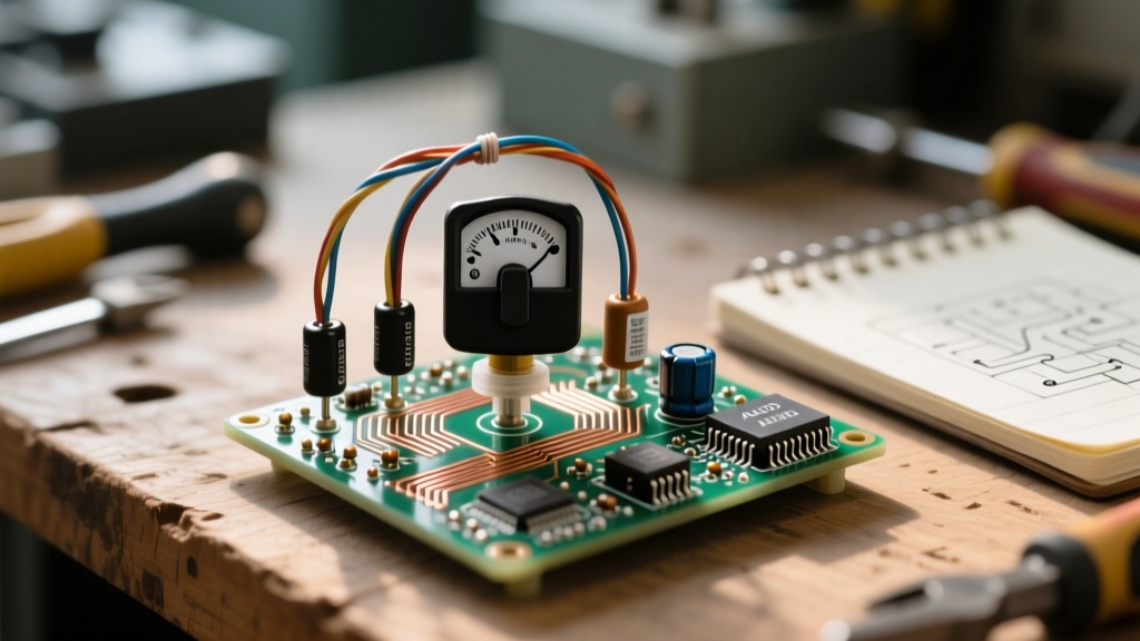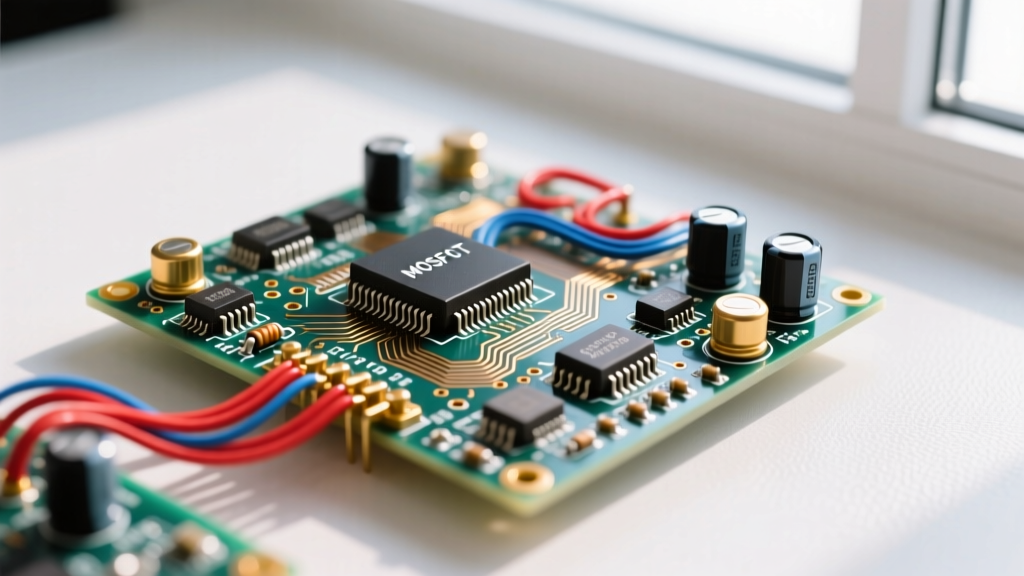

Building a MOSFET power amplifier offers distinct advantages over traditional Bipolar Junction Transistor (BJT) designs. MOSFETs provide exceptionally high input impedance, meaning they draw virtually zero current from the driver stage, and they lack the secondary breakdown mechanisms that plague BJTs under high-voltage, high-current conditions. However, designing a reliable audio or RF power amplifier with MOSFETs requires navigating a specific set of thermal and biasing traps. Most commercial power MOSFETs are optimized for high-frequency switching, not linear amplification, making proper component selection and thermal tracking mandatory for survival on the bench.
MOSFET Pinout, Symbol, and the Linear-Mode Trap
Before wiring up a power stage, you must understand the physical layout and the inherent body diode. A standard vertical power MOSFET (like the ubiquitous TO-220 or TO-247 packages) features three pins:
- Gate (G): The control terminal. It acts like a capacitor plate, insulated from the silicon by a microscopic layer of silicon dioxide. It requires voltage, not continuous current, to turn on.
- Drain (D): The primary current entry point (for N-channel). In a TO-220 package, the metal tab is almost always connected to the Drain.
- Source (S): The current exit point. This is your reference terminal for the Gate-Source voltage (Vgs).
Crucially, the physical structure of a vertical MOSFET creates an inherent parasitic body diode between the Source and Drain. In an N-channel device, the anode is at the Source and the cathode is at the Drain. If you wire a MOSFET power amplifier output stage incorrectly, this diode will conduct heavily during the negative half-cycle of your audio signal, destroying the device and your power supply.
Operation Regions and Safe Default Part Numbers
To use a MOSFET as an amplifier, you must bias it in the Saturation (or Active) region. This is highly counter-intuitive for engineers used to BJTs, where the 'saturation' region means the switch is fully ON. For a MOSFET, the fully-ON switching state is the Linear/Ohmic region.
| Region | Condition (N-Channel) | Behavior | Application |
|---|---|---|---|
| Cutoff | Vgs < Vgs(th) | Channel is closed. Only leakage current flows. | Switch (OFF state) |
| Linear / Ohmic | Vgs > Vgs(th) AND Vds < (Vgs - Vgs(th)) | Acts like a voltage-controlled resistor. Rds(on) is at its minimum. | Switch (ON state), PWM motor control |
| Saturation / Active | Vgs > Vgs(th) AND Vds > (Vgs - Vgs(th)) | Current (Id) is controlled by Vgs and is mostly independent of Vds. | Linear Power Amplification, Constant current sources |
Safe Default MOSFETs for Power Amplifiers
Not all MOSFETs survive linear mode. Modern 'trench' MOSFETs designed for DC-DC converters will suffer from the Spirito effect (thermal hotspotting) and self-destruct in seconds when used in linear audio amps. You must use older, planar HEXFET-style geometries. Below are the proven, safe defaults for DIY and prototype power amplifiers.
| Part Number | Type | Vds (Max) | Id (Cont) | Vgs(th) Range | Package | Linear Suitability |
|---|---|---|---|---|---|---|
| IRFP240 | N-Channel | 200V | 20A | 2.0V - 4.0V | TO-247 | Excellent (Planar die) |
| IRFP9240 | P-Channel | 200V | 12A | -2.0V - -4.0V | TO-247 | Excellent (Complementary pair) |
| IRF540N | N-Channel | 100V | 33A | 2.0V - 4.0V | TO-220 | Good (For <50W amps) |
| IRF9540 | P-Channel | 100V | 23A | -2.0V - -4.0V | TO-220 | Good (Complementary to IRF540N) |
A Practical 50W Class-AB MOSFET Power Amplifier Circuit
The most reliable topology for a hobbyist MOSFET power amplifier is a Class-AB complementary source-follower output stage. In this configuration, the MOSFETs provide current gain but no voltage gain (voltage gain is handled by the preceding driver stages). This minimizes distortion and keeps the MOSFETs operating safely within their Safe Operating Area (SOA).
Output Stage Component Values
Assuming a symmetrical ±35V DC power supply, here are the exact component values for a robust 50W into 8Ω output stage using the IRF540N and IRF9540 pair.
- Q1 (N-Channel Output): IRF540N
- Q2 (P-Channel Output): IRF9540
- R1, R2 (Gate Stoppers): 220Ω, 1/4W metal film. Mandatory to prevent parasitic RF oscillation.
- R3, R4 (Source Degeneration): 0.22Ω, 5W wirewound. Provides local negative feedback and forces current sharing.
- D1, D2 (Gate Protection): 15V, 1W Zener diodes (e.g., 1N4744A). Placed between Gate and Source (cathode to Gate for N-ch, anode to Gate for P-ch) to prevent Vgs from exceeding the ±20V absolute maximum.
- Q3 (Bias Spreader / Vbe Multiplier): BD139 (NPN). Mounted directly to the output heatsink.
- VR1 (Bias Trimpot): 10kΩ multi-turn cermet potentiometer.
- R5 (Bias Upper Leg): 1.2kΩ, 1/4W.
- R6 (Bias Lower Leg): 100Ω, 1/4W (in series with VR1).
Biasing for Quiescent Current and Thermal Tracking
Unlike BJTs, which have a negative temperature coefficient (they conduct more as they get hotter, leading to immediate thermal runaway), MOSFETs have a complex thermal profile. At high currents (above ~2A), they have a positive temperature coefficient, which is self-limiting and safe. However, at the low quiescent currents where a Class-AB amplifier idles, MOSFETs exhibit a negative temperature coefficient. If they get warm, their threshold voltage (Vgs(th)) drops, causing them to draw more idle current, which makes them hotter, dropping Vgs(th) further.
Step-by-Step Biasing Procedure
- Prepare the DMM: Set your multimeter to the DC millivolt (mV) range. Connect the probes across the N-channel source resistor (R3, the 0.22Ω wirewound).
- Cold Start: Power the amplifier with no load (disconnect the speaker) and no input signal. Turn the VR1 trimpot to its minimum resistance position. The DMM should read near 0mV (cutoff).
- Adjust Quiescent Current: Slowly turn VR1. Watch the DMM. Stop when you read 15mV to 20mV. By Ohm's law (I = V/R), 15mV across 0.22Ω equals ~68mA of quiescent bias current. This is the sweet spot to eliminate crossover distortion without overheating the TO-220 packages.
- Thermal Soak: Let the amplifier run for 15 minutes. The voltage will likely drift upward as the heatsink warms. Re-adjust VR1 back down to 15mV.
The Thermal Coupling Rule: The bias transistor (Q3, BD139) acts as a thermal sensor. It must be bolted to the exact same aluminum extrusion as Q1 and Q2, using thermal paste and an insulating mica pad. If Q3 is on the PCB, it will not sense the heatsink temperature, the bias voltage will not drop as the MOSFETs heat up, and your amplifier will enter thermal runaway and burn out.
Failure Modes and Multimeter Testing
When a MOSFET power amplifier fails, it is almost always due to one of three mechanisms: Gate oxide punch-through (from static discharge or exceeding ±20V Vgs), parasitic oscillation (missing gate stoppers), or SOA violation (driving a 2Ω load with a 4Ω designed amp, pushing the device out of its Safe Operating Area).
Testing a MOSFET out-of-circuit with a standard digital multimeter (DMM) is highly effective if you understand the limitations of the diode-test mode. Most DMMs output roughly 2.5V to 3.0V at the probes in diode mode.
How to Test an N-Channel MOSFET with a DMM
- Discharge the Gate: Short the Gate and Source pins together with a 10kΩ resistor or your finger. This bleeds off any trapped charge in the gate capacitance.
- Check the Body Diode: Set the DMM to Diode Test mode. Place the Red probe on the Source and the Black probe on the Drain. You should read a forward voltage drop of roughly 0.4V to 0.6V. Reverse the probes (Black on Source, Red on Drain); the meter should read 'OL' (Open Loop).
- Charge the Gate: Keep the Black probe on the Source. Momentarily touch the Red probe to the Gate. The DMM's internal 3V battery will charge the gate capacitance, turning the MOSFET on. Note: If the MOSFET has a Vgs(th) higher than 3.5V, your DMM might not fully turn it on. In that case, use a 9V battery with a 1kΩ resistor to briefly touch Gate to Source.
- Verify Conduction: Move the Red probe back to the Drain (Black remains on Source). The meter should now read a very low voltage drop (often 0.00V to 0.05V) or beep on continuity, indicating the channel is fully enhanced and conducting.
- Discharge and Verify Cutoff: Short Gate to Source again. Re-test Drain to Source; it should return to 'OL', proving the device can turn off and isn't shorted internally.
For deeper design theory and thermal stability calculations regarding lateral vs. vertical MOSFET geometries, Rod Elliott's comprehensive guide on MOSFET audio amplifiers remains the definitive reference for bench builders. Always consult the specific manufacturer datasheet for the SOA (Safe Operating Area) graph before finalizing your heatsink and power supply specifications.