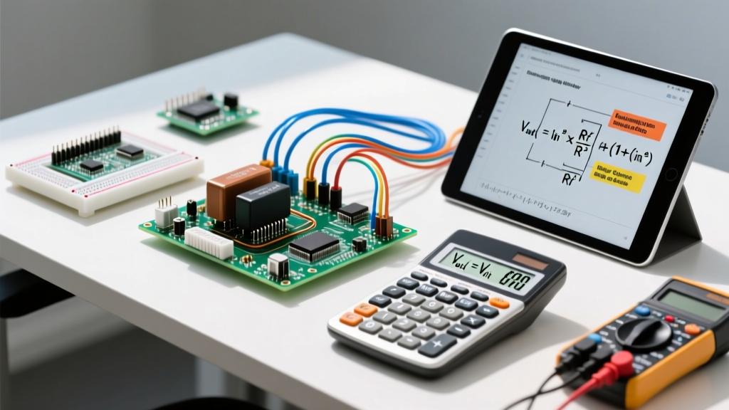
The non-inverting configuration is the workhorse of analog signal conditioning. When you need to amplify a high-impedance sensor signal without loading it down, an integrated circuit op amp wired in this topology provides near-infinite input impedance and a predictable, positive voltage gain. Unlike the inverting amplifier, the output signal maintains the same phase as the input, making it the default choice for audio preamps, strain gauge buffers, and DC precision measurement.
This guide walks through the exact node behavior, component selection, breadboard verification, and extreme failure modes of the non-inverting topology, using real-world bench parameters.
The Non-Inverting Topology: Node Labels and Core Behavior
To design this circuit, you must map the physical pins of your IC to the theoretical schematic nodes. Using the industry-standard 8-pin DIP package (like the TL072 or LM358), the node mapping for Channel A is:
- $V_{in}$ (Signal Input): Connects to Pin 3 (Non-inverting input, $V_+$).
- $V_{out}$ (Signal Output): Connects to Pin 1 (Output).
- $V_-$ (Inverting Input): Connects to Pin 2. This is the summing node where negative feedback is applied.
- $V_{CC}$ / $V_{EE}$ (Power Rails): Connect to Pin 8 (Positive) and Pin 4 (Negative/Ground).
The gain is set by two resistors: the feedback resistor ($R_f$) running from $V_{out}$ to $V_-$, and the ground resistor ($R_g$) running from $V_-$ to circuit ground. The closed-loop voltage gain ($A_v$) is calculated as:
$A_v = 1 + (R_f / R_g)$
Behavior Matrix: Element Variations
Understanding how component drift or deliberate changes affect the circuit is critical for debugging. Here is the behavior table for the non-inverting node network:
| Element Changed | Effect on Gain ($A_v$) | Effect on Bandwidth | Effect on Input Impedance |
|---|---|---|---|
| Increase $R_f$ | Increases | Decreases (Gain-Bandwidth Product limit) | No change (remains near-infinite) |
| Increase $R_g$ | Decreases (approaches 1) | Increases | No change |
| Increase $V_{in}$ | No change | No change | No change (until output clips) |
| Add Capacitor in series with $R_g$ | DC Gain becomes 1 (AC coupled) | Creates a high-pass filter corner | No change |
Component Selection and Design Walkthrough
Let us design a precision amplifier for a piezoelectric vibration sensor. The sensor outputs a 100mV peak-to-peak (p-p) AC signal and has a source impedance of 1MΩ. We need to amplify this to 1.1V p-p to feed a 3.3V microcontroller ADC safely.
Target Gain: $1.1V / 0.1V = 11$ (or 20.8 dB).
IC Selection: Texas Instruments TL072CP. It is a low-noise JFET-input dual op amp. Because it uses JFET inputs, its input bias current is in the picoamp range, meaning it will not load down our 1MΩ piezo sensor. A BJT-input op amp like the LM741 would draw nanoamps of bias current, creating a massive DC offset voltage across the sensor's internal resistance.
Calculating Real Component Values
We need $1 + (R_f / R_g) = 11$, which means $R_f / R_g = 10$. We must choose resistor values that are high enough not to waste current, but low enough to avoid excessive thermal noise and stray capacitance issues.
- $R_g$: 10kΩ (Standard E24 value)
- $R_f$: 100kΩ (Standard E24 value)
If you were using a BJT-input op amp (like the NE5532), you would need to place a compensation resistor ($R_{comp}$) in series with the non-inverting input to balance the voltage drops caused by input bias currents. $R_{comp}$ should equal the parallel combination of $R_f$ and $R_g$ ($100k || 10k = 9.09k\Omega$). Because we selected the JFET TL072, the bias current is negligible, and $R_{comp}$ is omitted to reduce Johnson-Nyquist thermal noise.
Breadboard Testing and Extreme Failure Modes
Theory falls apart if the physical layout introduces parasitic oscillation. Follow these numbered steps to breadboard and verify the circuit safely.
- De-energize the board. Insert the TL072 IC across the center trench of the breadboard.
- Wire the power rails. Connect Pin 8 to +12V DC and Pin 4 to -12V DC (or GND if using a split supply). Never exceed the absolute maximum supply voltage (±18V for the TL072).
- Install bypass capacitors. Place two 100nF (0.1µF) ceramic capacitors as close to the IC pins as physically possible: one from Pin 8 to GND, and one from Pin 4 to GND. This prevents high-frequency rail oscillation.
- Wire the feedback network. Insert the 10kΩ $R_g$ from Pin 2 to the GND rail. Insert the 100kΩ $R_f$ from Pin 2 to Pin 1.
- Connect the input. Wire your function generator or sensor signal to Pin 3 via a shielded cable to prevent 60Hz mains hum pickup.
- Power on and verify. Set your oscilloscope to AC coupling. Probe Pin 1. You should see a 1.1V p-p sine wave perfectly in phase with the 100mV input.
What Breaks at the Extremes? (Failure Mode Contrast)
When a component fails open or short on the jobsite, the integrated circuit op amp reacts in specific, predictable ways based on the loop gain equation.
| Failure State | Physical Result | Circuit Behavior |
|---|---|---|
| $R_f$ Opens | Feedback path broken. Pin 2 pulled to GND via $R_g$. | Op amp acts as an open-loop comparator. Output slams to the positive or negative rail depending on microvolt input offsets. |
| $R_f$ Shorts | Pin 2 tied directly to Pin 1. | Gain becomes exactly 1 ($1 + 0/R_g$). Circuit becomes a unity-gain buffer. Output mirrors input. |
| $R_g$ Opens | Pin 2 only connected to $R_f$. | No current flows through $R_f$. Therefore, no voltage drops across it. $V_-$ equals $V_{out}$. Circuit becomes a unity-gain buffer (Gain = 1). |
| $R_g$ Shorts | Pin 2 tied directly to GND. | Gain equation divides by zero. Infinite theoretical gain. Output immediately saturates to the positive supply rail. |
Why Non-Inverting Over Inverting?
Designers often default to the inverting topology because it provides a convenient 'virtual ground' at the summing node. However, the non-inverting integrated circuit op amp configuration wins in specific scenarios. Refer to the Analog Devices MT-041 Tutorial for deeper architectural comparisons.
| Criteria | Non-Inverting Topology | Inverting Topology |
|---|---|---|
| Input Impedance | Extremely High (Op amp common-mode impedance, often >10^12 Ω) | Low (Equal to the input resistor $R_{in}$) |
| Phase Shift | 0° (Output is in phase with input) | 180° (Output is inverted) |
| Minimum Gain | 1 (Unity gain buffer) | 0 (Attenuation possible) |
| Common-Mode Voltage | Varies with input signal (requires good CMRR) | Held at 0V (Virtual ground) |
Choose Non-Inverting when: You are interfacing with high-impedance sources (piezo pickups, pH probes, guitar pickups) where loading the source would destroy the signal amplitude.
Choose Inverting when: You need signal attenuation (gain < 1), or you are summing multiple signals in an audio mixer where the virtual ground prevents channel crosstalk.
Integrated Circuit Op Amp FAQ
Why is my integrated circuit op amp outputting a constant DC voltage instead of amplifying?
If your output is pegged to the positive or negative supply rail (saturation), you have lost negative feedback. Check $R_f$ and $R_g$ for cold solder joints or breadboard contact failures. If the feedback loop is physically intact, you may be violating the common-mode input voltage range. For example, if you are using a single-supply LM358 and feeding it an AC signal centered at 0V, the input drops below the negative rail, causing phase reversal or saturation. You must bias the non-inverting pin to mid-supply (VCC/2) for single-supply AC operation.
Can I use a single-supply integrated circuit op amp for AC audio signals?
Yes, but you must create an artificial ground. Op amps like the TL072 require a dual supply (e.g., ±12V) to handle signals that swing above and below 0V. If you only have a single 9V battery, use an IC specifically rated for single-supply rail-to-rail input/output (RRIO), such as the MCP6002. You must then use a voltage divider (two equal resistors, e.g., 100kΩ each) to bias the non-inverting input to 4.5V, and AC-couple your input and output signals with series capacitors to block the DC bias.
What causes high-frequency oscillation in an integrated circuit op amp circuit?
Oscillation (often visible as a thick, fuzzy trace on an oscilloscope or excessive heat on the IC) is caused by degraded phase margin. The three most common bench culprits are: 1. Missing or poorly placed power supply bypass capacitors. 2. Driving a heavy capacitive load (like a long coaxial cable) directly from the output pin without a series isolation resistor (typically 22Ω to 100Ω). 3. Using feedback resistors that are too large (e.g., >1MΩ), which interact with the op amp's internal parasitic input capacitance to create an unintended low-pass filter in the feedback path, adding destructive phase shift.