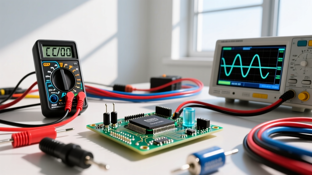
Transitioning from a working breadboard prototype to a manufactured printed circuit board is where many hardware projects stall. When you design a PCB board, you are no longer just connecting logic gates; you are managing parasitic inductance, thermal dissipation, and current density. A circuit that behaves perfectly on a solderless breadboard can oscillate, overheat, or fail to start once laid out in copper. This guide provides the exact trace sizing data, migration checklists, and first-spin testing protocols needed to ensure your first board revision powers up cleanly.
The Breadboard-to-PCB Migration Checklist
Breadboards are excellent for validating logic, but they introduce massive parasitic variables. Adjacent breadboard rows typically share 2pF to 5pF of capacitance, and the long jumper wires act as inductors. If you blindly copy a breadboard schematic into your CAD software without adjusting for physical layout, these mistakes will survive the transition:
On a breadboard, the high inductance of jumper wires often masks high-frequency switching noise because the wires themselves act as low-pass filters. When you route tight, low-inductance traces on a PCB, fast-switching ICs (like 74HC logic or switching regulators) will inject massive ground bounce into your rails unless local decoupling is implemented correctly.
Use this numbered checklist before finalizing your schematic for layout:
- Implement Local Decoupling: Place a 100nF (X7R ceramic) capacitor physically adjacent to every VCC/GND pin pair on every IC. Add a 10µF to 47µF bulk tantalum or electrolytic capacitor at the main power entry point.
- Eliminate Ground Daisy-Chains: Never route ground returns in a daisy-chain topology. Use a continuous copper ground plane on Layer 2 (for 2-layer boards) or Layer 3 (for 4-layer boards) to provide a low-impedance return path directly beneath the signal trace.
- Terminate Floating Inputs: Breadboard leakage currents can sometimes bias floating CMOS inputs into a stable state. On a clean FR4 PCB, those same inputs will oscillate, drawing massive quiescent current. Add 10kΩ pull-up or pull-down resistors to all unused logic gates and microcontroller pins.
- Separate Analog and Digital Domains: Route digital return currents away from sensitive analog nodes (like ADC references or op-amp inputs). Use a split ground plane or careful component placement to keep high di/dt digital currents out of the analog ground path.
Trace Width vs. Current: Sizing Your Copper
The most common physical failure on a first-spin board is a trace that acts as a fuse. To determine what trace width a specific current needs, you must account for the copper weight (thickness), the allowable temperature rise, and whether the trace is on an external or internal layer. Internal layers dissipate heat poorly and typically require twice the width of external layers for the same current.
The industry standard for this calculation is IPC-2221 (and the updated IPC-2152). Below is a reference table for external layer traces based on a 10°C temperature rise above ambient.
| Current (Amps) | 1 oz Copper (External) | 2 oz Copper (External) | Typical Application |
|---|---|---|---|
| 1.0 A | 10 mils (0.25 mm) | 6 mils (0.15 mm) | Signal lines, small sensors |
| 2.0 A | 25 mils (0.64 mm) | 12 mils (0.30 mm) | USB power, small servos |
| 3.0 A | 50 mils (1.27 mm) | 25 mils (0.64 mm) | Stepper motors, LED strips |
| 5.0 A | 110 mils (2.79 mm) | 55 mils (1.40 mm) | DC-DC converters, BLDC phases |
| 10.0 A | 300 mils (7.62 mm) | 150 mils (3.81 mm) | Main battery feeders, inverters |
Note: For internal layers, double the recommended trace width. For precise calculations accounting for specific board thicknesses and copper pours, use the All About Circuits Trace Width Calculator or the Saturn PCB Toolkit.
Workshop Safety: Soldering Alloys and Fume Extraction
Assembling your first prototype by hand requires strict attention to metallurgy and ventilation. The flux core inside your solder wire vaporizes at high temperatures, releasing colophony (rosin) fumes that are a known respiratory sensitizer and can cause occupational asthma.
Alloy Selection and Tip Temperatures
Your iron temperature must be matched to the alloy's melting point, not set arbitrarily high. Excessive heat burns the flux core before it can wet the pad, resulting in cold, grainy joints.
- Leaded (Sn63/Pb37): Eutectic melting point is 183°C. Set your iron to 320°C - 340°C. Ideal for hobbyist prototyping due to superior wetting and shiny joint inspection. Requires strict hand-washing and separate workspace from food.
- Lead-Free (SAC305 - Sn96.5/Ag3.0/Cu0.5): Melting point is 217°C. Set your iron to 350°C - 370°C. Mandatory for commercial production (RoHS compliance). Requires a higher-wattage iron (70W+) to maintain thermal recovery on large ground planes.
Testing Your First-Spin Board
When the bare boards arrive and assembly is complete, do not immediately connect a battery or an unregulated wall adapter. A systematic power-up sequence prevents catastrophic failures and isolates faults safely.
- Visual Inspection (10x Loupe): Inspect all SMD pads for solder bridges, tombstoning, and missed pins. Check through-hole components for cold joints and verify polarity on electrolytic capacitors and diodes.
- Short Circuit Verification: Set your digital multimeter (DMM) to continuity or diode mode. Measure between VCC and GND, and between any regulated voltage rail (e.g., 3.3V) and GND. You should read a high impedance or a slow-charging capacitance curve, not a dead short (< 5 ohms).
- Current-Limited Power-Up: Connect a benchtop power supply set to the nominal voltage, but limit the current to 50mA - 100mA. If the board hits the current limit immediately and the voltage sags, power down and hunt for a short or a backward-oriented polarized component.
- Thermal Imaging: While the board is powered under current limiting, scan it with a thermal camera (like a FLIR ONE or InfiRay). Look for localized hotspots on ICs, resistors, or vias that indicate a hidden short or a leaking capacitor.
- Signal Injection: Once rails are verified stable, remove the current limit, power up fully, and use an oscilloscope to probe clock signals, enable pins, and communication buses (I2C/SPI) to verify logic levels and edge rates.
Frequently Asked Questions
What is the minimum trace width I should use when I design a PCB board?
Most standard overseas fab houses (like JLCPCB or PCBWay) advertise a minimum trace width and spacing of 3.5 to 4 mils (0.09mm) for advanced tiers, but their standard process reliably handles 6 mils (0.15mm). For optimal yield and to prevent etching defects that could lead to open circuits, aim for a minimum of 8 to 10 mils for signal traces unless you are routing high-density BGA fanouts.
How do I calculate via current capacity when I design a PCB board?
A via's current capacity is determined by its drill diameter and the plating thickness (typically 1 mil or 25µm for standard processes). As a rule of thumb based on IPC-2152, a single standard 0.3mm (12 mil) drill via with 1 mil plating can safely carry about 1 Amp with a 10°C temperature rise. For high-current paths, never rely on a single via; use an array of 4 to 8 vias in parallel to transition between layers, which also reduces the total via inductance.
Why does my PCB overheat even though the traces are wide enough?
If your traces are sized correctly per IPC-2221 but the board still runs hot, the issue is usually thermal dissipation, not electrical resistance. First, verify you actually ordered the copper weight you designed for (e.g., ordering 1oz when you calculated for 2oz). Second, check for skin effect if you are running high-frequency AC or PWM; high frequencies travel only on the surface of the copper, effectively reducing the cross-sectional area. Finally, ensure you have placed thermal vias under the exposed pads of SMD power components to conduct heat into the internal ground planes.