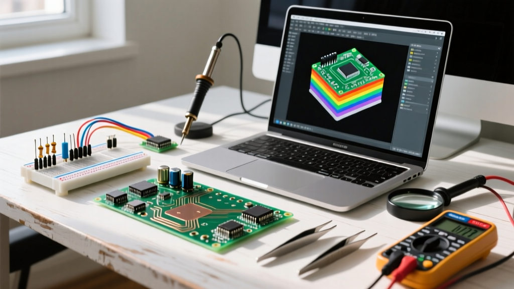

Transitioning from a breadboard prototype to a manufactured printed circuit board (PCB) is the most critical leap in hardware development. Learning how to design a PCB at home requires more than just drawing lines between pads; it demands translating breadboard parasitics into a robust schematic, routing traces based on IPC-2221 current standards, and validating the bare board before applying power. This guide provides the exact engineering parameters, safety protocols, and testing sequences required for a successful first-spin board.
The Breadboard-to-PCB Migration Checklist
Breadboards are excellent for logic verification but terrible for final circuit validation. A standard solderless breadboard introduces 2-5 pF of parasitic capacitance per contact and exhibits contact resistance ranging from 100 mΩ to over 500 mΩ. When you move to a PCB, these hidden parasitics vanish, often causing high-speed oscillations or power rail sag that the breadboard was accidentally masking.
Follow this migration checklist to ensure your design survives the transition:
- Redraw the schematic from scratch: Do not rely on your breadboard spaghetti wiring. Re-enter the schematic in your EDA tool (like KiCad or Altium) to catch missing connections.
- Add local decoupling capacitors: Place a 100 nF (0.1 µF) X7R ceramic capacitor within 2 mm of every IC VCC pin, routed directly to the ground plane. Breadboards hide the need for these by acting as accidental low-pass filters.
- Eliminate ground loops: Replace daisy-chained ground wires with a continuous copper ground plane on Layer 2 (or Layer 4 for 4-layer boards).
- Account for high-di/dt loops: Keep the physical loop area between switching components (like MOSFETs), freewheeling diodes, and bulk capacitors as tight as possible to minimize radiated EMI.
The most common mistakes that survive from breadboard to PCB are floating CMOS inputs, inadequate ground return paths for high-current loads, and missing flyback diodes on relay coils. Always run an Electrical Rules Check (ERC) in your EDA software before generating Gerber files to catch unconnected pins.
Sizing Your Traces: Current, Copper Weight, and Thermals
Determining what trace width a specific current needs is governed by the IPC-2221 standard. The required width depends on the copper weight (thickness), the allowable temperature rise, and whether the trace is on an external or internal layer. Internal layers have roughly half the heat dissipation capacity of external layers, requiring twice the width for the same current.
The table below provides baseline trace widths for external layers with a standard 10°C temperature rise above ambient. For precise calculations accounting for specific board thicknesses and copper weights, use the Saturn PCB Toolkit or the All About Circuits Trace Width Calculator.
| Target Current (A) | 1 oz Cu (35 µm) Width (mil) | 1 oz Cu (35 µm) Width (mm) | 2 oz Cu (70 µm) Width (mil) | 2 oz Cu (70 µm) Width (mm) |
|---|---|---|---|---|
| 0.5 A | 10.5 | 0.27 | 6.0 | 0.15 |
| 1.0 A | 20.0 | 0.51 | 11.0 | 0.28 |
| 2.0 A | 50.0 | 1.27 | 25.0 | 0.64 |
| 3.0 A | 80.0 | 2.03 | 40.0 | 1.02 |
| 5.0 A | 150.0 | 3.81 | 75.0 | 1.91 |
Note: If your home PCB design uses 0.5 oz copper (common in cheap rapid-prototyping services), you must double the 1 oz width values listed above to maintain the same thermal performance.
Workshop Safety and Soldering Specifics
Designing the board is only half the battle; assembling it at home requires strict adherence to thermal and chemical safety protocols. Soldering generates particulate matter and vaporized flux that can cause occupational asthma and contact dermatitis.
Fume Extraction and Alloy Selection
Never solder in a stagnant room. Use a dedicated fume extractor equipped with both a HEPA filter (for particulates) and an activated carbon filter (for volatile organic compounds from rosin flux). A unit like the Hakko FA-400 or a DIY blower box with replacement carbon mats is mandatory for enclosed home workshops.
Select your solder alloy based on your component density and thermal tolerance:
- Sn63Pb37 (Leaded Eutectic): Melts sharply at 183°C. Ideal for home DIY, through-hole, and basic SMD work. It wets easily and produces shiny, reliable joints.
- SAC305 (Lead-Free): Melts at 217°C - 220°C. Required for RoHS-compliant commercial designs but requires higher iron temperatures and more aggressive flux, increasing the risk of lifting FR4 pads.
Iron Temperature and Tip Maintenance
For Sn63Pb37 solder with a standard rosin-core (RMA) flux, set your soldering station (e.g., Hakko FX-888D or Pine64 Pinecil) to 320°C - 350°C. Use a chisel tip (like the T18-D24) for maximum thermal transfer to ground planes. Do not exceed 380°C; excessive heat burns the flux core before it can clean the oxidation off the pad, resulting in cold, grainy joints and degraded fiberglass substrates. Always tin the tip with fresh solder before placing it back in the holder to prevent oxidation.
Testing Your First Spin Board
When your bare PCB arrives from the fab house and you have populated the components, do not simply plug it into a wall adapter. A systematic power-up sequence prevents catastrophic failure of expensive ICs.
- Visual Inspection: Use a 10x jeweler's loupe or a digital microscope to inspect all SMD pads and through-hole joints for solder bridges, especially under QFN and SOIC packages.
- Short Circuit Validation: Set your multimeter to continuity mode. Place the black probe on the main ground plane and the red probe on every VCC rail. The meter must read OL (Open Loop) or show a high resistance that slowly climbs (indicating capacitor charging). If it reads less than 10 ohms, you have a solder bridge or a backwards polarized capacitor. Do not proceed.
- Current-Limited Power Up: Connect a bench power supply (like a Rigol DP832 or Korad KA3005P) set to your target voltage. Crucially, set the current limit (OCP) to 50 mA. Power the board. If the supply hits the 50 mA limit and the voltage sags, you have a fault. If the board draws 15 mA and the voltage holds steady, proceed.
- Rail Validation: With the board powered, use your multimeter to probe the VCC pin of every major IC. Verify that voltage drops across ferrite beads or LDOs are within datasheet specifications.
- Signal Injection: Once power rails are validated, inject your first logic signal or clock and verify the output with an oscilloscope, checking for clean rise times and absence of ground bounce.
Frequently Asked Questions
What is the most cost-effective software to design a PCB at home?
For home designers and hobbyists, KiCad is the undisputed standard. It is completely free, open-source, and imposes no artificial limits on schematic size, layer count, or pin numbers. The integrated 3D viewer allows you to check mechanical clearances before ordering, and the active community provides extensive third-party symbol and footprint libraries. Unlike freemium alternatives, KiCad does not hold your design files hostage behind a paywall when you are ready to generate manufacturing files.
How do I calculate via current capacity for my home PCB?
Vias are essentially tiny plated barrels connecting layers. A standard via with a 0.3 mm drill diameter and 0.6 mm pad size, plated with 1 oz (approx. 20-25 µm) copper, can safely carry about 0.5 A with a 10°C temperature rise. If you need to route 3 A to an inner layer, do not rely on a single via. Instead, use an array of three to four vias in parallel (a "via stitching" pattern) to distribute the current and reduce the thermal bottleneck. Always keep high-current vias away from the edges of pads to prevent solder wicking during reflow.
Why did my DIY PCB etchant eat through the copper completely?
If you are etching PCBs at home using the toner transfer method and ferric chloride or sodium persulfate, over-etching usually occurs due to poor toner adhesion or exhausted etchant. Ensure you are using yellow, toner-heavy paper (like glossy magazine pages) and press the iron evenly at the cotton setting (approx. 180°C). More importantly, etchant solutions lose efficacy as they become saturated with dissolved copper. If the etching process takes longer than 20 minutes with constant agitation, your solution is likely depleted, causing it to attack the edges of your toner mask (undercutting) and destroy fine traces. Always mix fresh etchant for critical, high-density boards.


