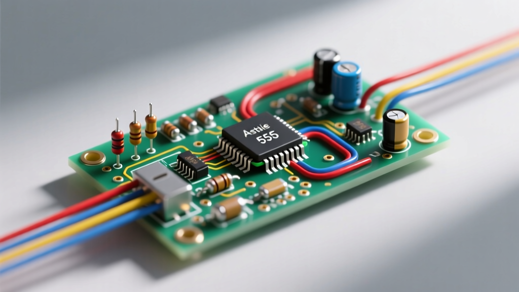

The classic astable IC 555 circuit diagram generates a continuous square wave by charging and discharging a timing capacitor through two resistors. Unlike monostable (one-shot) configurations, the astable topology requires no external trigger to start; it oscillates freely the moment power is applied. For a standard bipolar NE555 operating between 4.5V and 16V, the output (Pin 3) swings from roughly 1.7V above ground to 1.7V below VCC, sourcing or sinking up to 200mA. If you need rail-to-rail output and lower quiescent current, swap the bipolar chip for a CMOS variant like the TLC555 or LMC555.
The Astable Topology: Node Labels and Current Paths
To debug or design this circuit, you must understand the internal voltage dividers and how the external components interact with the 8-pin DIP package. The internal block diagram features three 5kΩ resistors creating reference voltages at 1/3 VCC and 2/3 VCC.
- Node A (VCC / GND): Pin 8 connects to the positive supply (4.5V–16V for NE555). Pin 1 connects to system ground. A 10µF to 100µF decoupling capacitor must bridge these pins as close to the IC as possible to suppress transient current spikes during output switching.
- Node B (Timing / Discharge Junction): Pins 6 (Threshold) and 7 (Discharge) tie together at the junction of resistors R_A and R_B. Pin 7 contains an internal open-collector NPN transistor that pulls this node to ground when the output is low.
- Node C (Trigger / Capacitor Junction): Pin 2 (Trigger) ties to the junction of R_B and the timing capacitor C_1. This node monitors the capacitor voltage against the internal 1/3 VCC reference.
- Node D (Control Voltage): Pin 5 provides access to the 2/3 VCC reference. In 95% of astable designs, you bypass this to ground with a 10nF ceramic capacitor to reject high-frequency noise. If you inject a varying voltage here, you create a voltage-controlled oscillator (VCO).
- Node E (Reset): Pin 4 is active-low. It must be tied directly to VCC (Node A) for normal operation. Pulling it below 0.7V forces the output low and halts oscillation.
Component Selection and Behavior Matrix
The oscillation frequency and duty cycle are dictated by the RC time constants. The governing equations are:
- Frequency:
f = 1.44 / ((R_A + 2 * R_B) * C_1) - Time High:
t_high = 0.693 * (R_A + R_B) * C_1 - Time Low:
t_low = 0.693 * R_B * C_1 - Duty Cycle:
D = (R_A + R_B) / (R_A + 2 * R_B)
Below is a data-dense matrix using standard E24 series component values for common target frequencies. These values assume an ideal capacitor; in practice, electrolytic capacitors (used for lower frequencies) have a ±20% tolerance, so expect real-world frequencies to drift accordingly.
| Target Freq | C_1 (Capacitor) | R_A (Resistor) | R_B (Resistor) | Actual Freq | Duty Cycle |
|---|---|---|---|---|---|
| 1 Hz | 10 µF (Electrolytic) | 47 kΩ | 47 kΩ | 1.02 Hz | 66.6% |
| 10 Hz | 1 µF (Ceramic/Film) | 47 kΩ | 47 kΩ | 10.2 Hz | 66.6% |
| 1 kHz | 10 nF (Ceramic) | 4.7 kΩ | 4.7 kΩ | 1.02 kHz | 66.6% |
| 10 kHz | 1 nF (Ceramic) | 4.7 kΩ | 4.7 kΩ | 10.2 kHz | 66.6% |
| 38 kHz (IR) | 470 pF (Ceramic) | 15 kΩ | 33 kΩ | 37.7 kHz | 59.2% |
t_high includes both R_A and R_B, while t_low only includes R_B. To achieve exactly 50%, place a signal diode (like a 1N4148) in parallel with R_B, with the cathode facing VCC. This bypasses R_B during the charging phase.
Behavior Matrix: Parameter Sensitivity
Understanding how the circuit reacts to component drift is critical for precision timing applications.
| Parameter Changed | Effect on Frequency | Effect on Duty Cycle | Effect on Power Draw |
|---|---|---|---|
| Increase R_A | Decreases | Increases (approaches 100%) | Negligible change |
| Increase R_B | Decreases | Decreases (approaches 50%) | Negligible change |
| Increase C_1 | Decreases | No change | Negligible change |
| Increase VCC | No change (ideally) | No change | Increases (quiescent current rises) |
Design Walkthrough: Building a 10 Hz Pulse Generator
Let us design a visible LED flasher running at roughly 10 Hz. We will use a 5V supply and a standard NE555P.
- Select C_1: Choose a 1µF ceramic capacitor (X7R dielectric, 50V rated). Ceramic is preferred over electrolytic here to avoid equivalent series resistance (ESR) timing errors.
- Calculate Total Resistance: Using
R_total = 1.44 / (f * C_1), we get1.44 / (10 * 0.000001) = 144,000 Ω(144 kΩ). - Assign R_A and R_B: We know
R_A + 2*R_B = 144 kΩ. If we pick standard E24 values of R_A = 47 kΩ and R_B = 47 kΩ, our total is47 + 94 = 141 kΩ. - Verify Frequency:
f = 1.44 / (141,000 * 0.000001) = 10.21 Hz. This is well within acceptable tolerance for a visual indicator. - Calculate Current Limiting for LED: The NE555 output (Pin 3) high state is roughly VCC - 1.7V = 3.3V. For a standard red LED (Vf = 2.0V, If = 20mA), the series resistor should be
R = (3.3V - 2.0V) / 0.02A = 65 Ω. Use the next standard E24 value up: 68 Ω.
Failure Modes: What Breaks at the Extremes?
Bench troubleshooting requires knowing exactly how the circuit fails when a solder joint cracks or a component shorts. Consult the Texas Instruments NE555 Datasheet for internal schematic references.
- R_A Shorts: Catastrophic failure. When the internal discharge transistor turns on, it connects Pin 7 to ground. If R_A is shorted, VCC is connected directly to ground through this internal transistor. The silicon will overheat and destroy the IC in milliseconds. Always use a minimum R_A value of 1kΩ to limit discharge current.
- R_B Opens: The timing capacitor C_1 can no longer charge toward VCC. Pin 6 (Threshold) never reaches 2/3 VCC. The internal flip-flop remains set, and the output (Pin 3) stays permanently HIGH.
- C_1 Shorts: Pin 2 (Trigger) is pulled directly to ground. Since 0V is always less than the 1/3 VCC threshold, the internal comparator continuously resets the flip-flop. The output stays permanently HIGH (wait, if trigger is low, it sets the output HIGH and turns off discharge. Since C1 is shorted, threshold is also 0V, which is < 2/3 VCC, so it doesn't reset. Output remains HIGH).
- Pin 5 (Control) Left Floating: The 2/3 VCC reference becomes susceptible to ambient electromagnetic interference. The frequency will jitter wildly, or the circuit may fail to oscillate entirely. Always use a 10nF bypass capacitor to ground.
Why the 555 Over Discrete Transistors or MCU PWM?
With microcontrollers like the ESP32 or Arduino Nano costing under $5, why use a 50-year-old timer IC? The decision hinges on boot time, hardware complexity, and brownout resilience. For a deeper look at digital alternatives, review this guide on 555 astable operation vs digital logic.
| Criterion | 555 Astable | Discrete BJT Astable | MCU PWM (e.g., ESP32) |
|---|---|---|---|
| Component Count | 1 IC, 2 R, 1 C (Low) | 2 BJTs, 4 R, 2 C (High) | 1 MCU, decoupling (Medium) |
| Time to First Pulse | Instant (µs) | Instant (µs) | Delayed (Bootloader + Code init) |
| Brownout Behavior | Stops, resumes instantly | Stops, resumes instantly | Requires full reboot/re-init |
| Duty Cycle Flexibility | Fixed by hardware (needs diode mod for 50%) | Fixed by hardware | Software-defined (0.1% resolution) |
| High Current Drive | 200mA (Direct LED/Relay drive) | Requires MOSFET/Relay | Requires MOSFET (GPIO limits ~40mA) |
Step-by-Step Breadboard Verification
Do not just wire the circuit and apply power. Follow this systematic verification sequence to catch wiring errors before they melt your breadboard.
- Power Off - Continuity Check: With the power supply disconnected, set your digital multimeter (DMM) to continuity mode. Place the black probe on the ground rail and the red probe on Pin 1. You should hear a beep. Check Pin 8 to VCC rail. Verify there is no short between VCC and GND rails.
- Verify Reset and Control Pins: Ensure Pin 4 (Reset) is jumpered directly to the VCC rail. Ensure Pin 5 (Control) has a 10nF ceramic capacitor connected to ground. Missing either of these guarantees erratic behavior.
- Apply Power - Quiescent Check: Set your bench power supply to 5.0V with a current limit of 100mA. Apply power. The DMM should read between 3mA and 10mA (the quiescent current of the bipolar NE555). If it spikes to the 100mA limit, immediately cut power; you have a short or a backwards IC.
- Measure DC Bias: Use the DMM in DC voltage mode. Measure Pin 3 (Output). It should read either ~3.3V (High) or ~0.2V (Low). If it reads ~2.5V, the circuit is not oscillating and is stuck in a linear/undefined state.
- Frequency Verification: Switch your DMM to the Frequency (Hz) mode. Probe Pin 3. You should read your target frequency (e.g., 10.2 Hz). If your DMM lacks a frequency mode, switch to an oscilloscope.
- Oscilloscope Sawtooth Check: Connect the scope probe to Pin 6 (Threshold). You should see a clean sawtooth wave ramping from 1.66V (1/3 VCC) to 3.33V (2/3 VCC). If the waveform is jagged or shows high-frequency ringing, your breadboard parasitic capacitance or long jumper wires are introducing noise; shorten the leads and verify the Pin 5 bypass capacitor.
By treating the IC 555 not as a magic black box but as a network of comparators and flip-flops governed by RC time constants, you can reliably design, debug, and scale astable oscillators for everything from simple LED flashers to ultrasonic transducers.


