
The Reverse Engineering Mindset: Why Trace a PCB?
Converting a physical printed circuit board into a readable schematic is one of the most rewarding skill paths in electronics. Whether you are repairing legacy industrial equipment, analyzing a competitor's commercial product, or simply trying to understand a clever open-source hardware design, mastering the transition from a physical pcb to circuit diagram requires a systematic, disciplined approach. Unlike designing from scratch, reverse engineering demands that you act as a detective, piecing together the original designer's intent from copper traces, vias, and component placements. This guide outlines a progressive skill-building path, taking you from basic visual teardowns to advanced netlist extraction and EDA (Electronic Design Automation) drafting.
Phase 1: Visual Documentation and Teardown (Beginner)
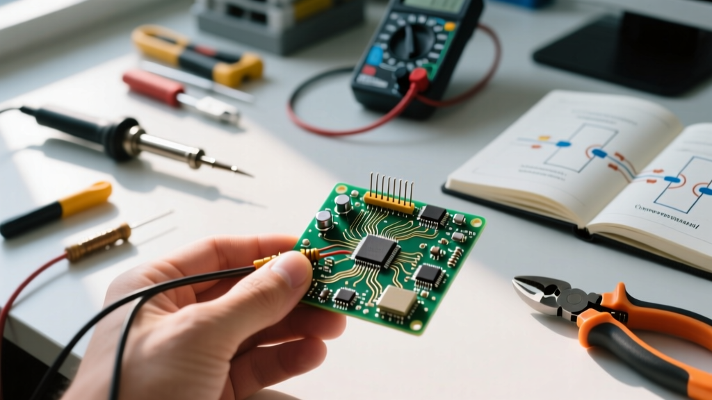
Before you ever touch a multimeter probe to the board, you must create a flawless visual archive. Once a component is desoldered or a trace is scratched, that physical evidence is gone forever.
Cleaning and Preparation
Begin by cleaning the board with 99% Isopropyl Alcohol (IPA) and an ESD-safe soft-bristle brush. This removes flux residue, dust, and grime that can obscure fine SMD (Surface Mount Device) markings and hairline traces. Avoid using lower concentration alcohols, as the water content can leave mineral deposits that interfere with later continuity testing.
Macro Photography and Component Mapping
Use a macro lens or a high-quality digital microscope to capture overlapping, high-resolution images of both the top and bottom layers. Pro-Tip: Place a circular polarizing filter over your light source and camera lens. This eliminates the harsh glare from HASL (Hot Air Solder Leveling) or ENIG (Electroless Nickel Immersion Gold) finishes, revealing the underlying silk screen and trace routing. Import these images into an image editor like GIMP or Photoshop, mirror the bottom layer so it aligns with the top layer, and reduce the opacity to 50%. This creates a digital 'X-ray' view of the board.
Next, catalog every component. For SMD resistors and capacitors, you will need an LCR meter to measure values if the silkscreen is missing. For active components, use an SMD codebook app (like the one by Mars Technologies) to decode the 2- or 3-character markings on transistors and diodes. For example, a marking of 'A7' on a SOT-23 package typically indicates a BAV99 dual switching diode.
Phase 2: Continuity Tracing and Net Mapping (Intermediate)
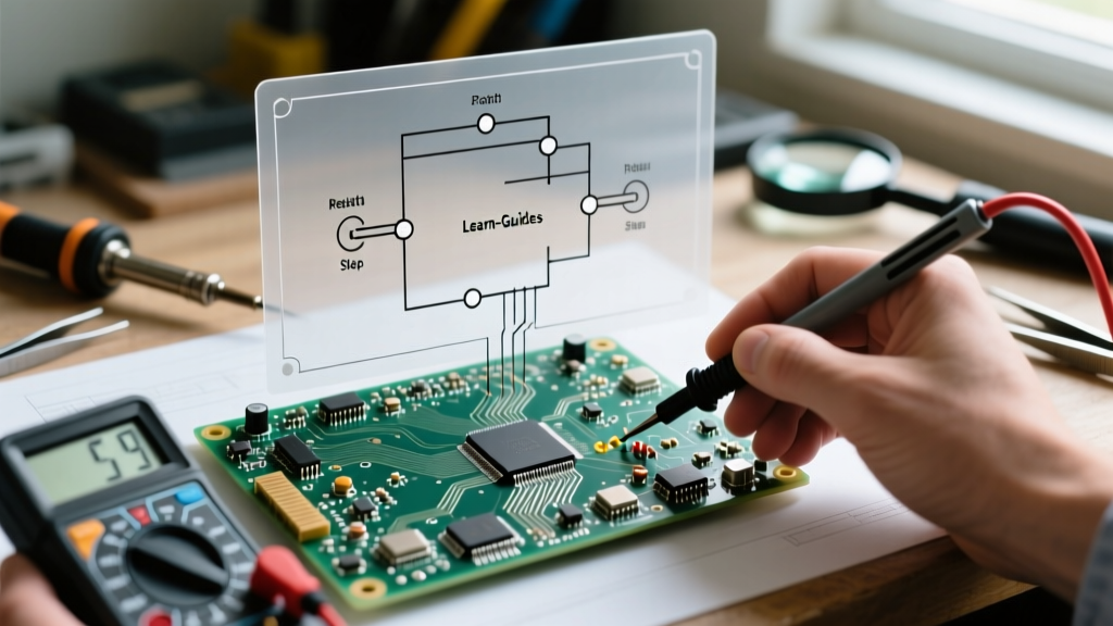
With your visual map complete, it is time to extract the electrical connections. This phase bridges the physical hardware and the logical schematic.
Selecting the Right Multimeter
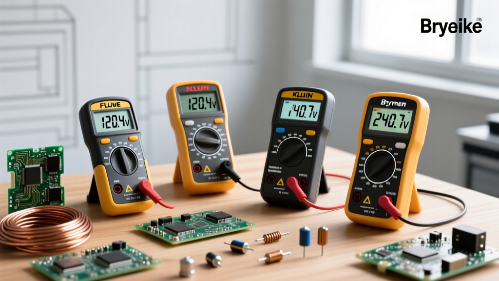
Standard multimeters often have a continuity threshold that is too slow or inaccurate for dense PCB tracing. You need a meter with a fast, latching continuity beeper. The Brymen BM235 or the Fluke 87V are industry favorites because their acoustic response is nearly instantaneous, allowing you to 'buzz out' a netlist rapidly without waiting for the screen to update. Use sharp, needle-point test probes; standard blunt probes will slip off 0402 or 0603 component pads.
The Ground Plane and Scratch-and-Probe Technique
Always start by identifying the main Ground (GND) plane. On a 2-layer board, this is usually the largest continuous copper pour. Map out the GND net first, as it will connect to the cathode of bypass capacitors, the ground pins of ICs, and the negative terminals of power inputs.
Field Technique: When traces disappear into vias covered by solder mask, use a fiberglass scratch pen or a fine sewing needle to gently scrape away the mask over the via annular ring. This exposes bare copper, giving your needle probe a reliable contact point for continuity testing without damaging the underlying trace.
Work systematically from the power input section outward. Map the power rails (e.g., 5V, 3.3V, 1.8V) by probing the input and output pins of voltage regulators (LDOs or switching buck converters). Document these nets on a physical notepad or a spreadsheet before moving to the EDA software.
Phase 3: Schematic Drafting in EDA Software (Advanced)
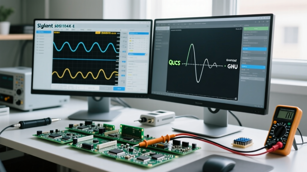
Translating your raw netlist data into a professional schematic requires proficiency in EDA tools. KiCad's Eeschema is the premier open-source choice for this task, offering powerful features specifically suited for reverse engineering.
Hierarchical Sheets and Logical Grouping
Do not attempt to draw a complex commercial PCB on a single schematic sheet. Utilize KiCad's hierarchical sheet feature to break the circuit down into logical functional blocks: Power Management, Microcontroller/DSP Core, Analog Front End, and I/O Interfaces. This mirrors how professional engineers design boards and makes the resulting diagram infinitely easier to read and troubleshoot.
Netlist Highlighting and Verification
As you place symbols and draw wires, use the 'Highlight Net' feature. Click on a net label (e.g., I2C_SDA) and verify that the highlight matches the physical nodes you mapped during Phase 2. For complex ICs, download the manufacturer's datasheet and use their 'Typical Application Circuit' as a reference skeleton, modifying it to match the specific passive component values you measured on the physical board.
Tool Matrix: Essential Gear for PCB Tracing
Investing in the right tools drastically reduces the time required to convert a pcb to circuit diagram format. Below is a comparison of essential hardware for the reverse engineering workbench.
| Tool Category | Recommended Model | Primary Purpose | Estimated Price (USD) |
|---|---|---|---|
| Digital Multimeter | Brymen BM235 | Fast continuity beeping, precise mV measurements for shunt resistors. | $110 - $130 |
| LCR Meter | DER EE DE-5000 | Measuring unmarked SMD capacitors and inductors with high accuracy. | $90 - $110 |
| Digital Microscope | AmScope SM-4TZ | Trinocular stereo zoom for reading microscopic SMD silkscreen codes. | $350 - $450 |
| Soldering Station | Pine64 Pinecil V2 | Precision desoldering of ICs using hot air or fine-tip rework. | $25 - $40 |
| Logic Analyzer | Saleae Logic Pro 16 | Capturing digital bus traffic to infer MCU pinout functions. | $399+ |
Overcoming Multi-Layer Board Limitations
The skill path hits a major bottleneck when transitioning from 2-layer hobbyist boards to 4, 6, or 8-layer commercial designs. In multi-layer boards, the inner layers are typically dedicated to solid ground and power planes, but high-density designs often route high-speed signals (like DDR memory buses or USB differential pairs) on inner layers using blind and buried vias.
Without destructive testing, tracing inner signal layers is nearly impossible. Advanced reverse engineering labs use X-ray inspection or carefully sand down the board layer-by-layer (delamination), taking macro photos at each stage. For the independent engineer, the best approach is to rely on the 'Typical Application' circuits in the datasheets of the main ICs. By assuming the inner layers follow the manufacturer's strict impedance and routing guidelines, you can accurately reconstruct 80% of the schematic without ever seeing the hidden copper.
Authoritative Resources for Further Study
To deepen your expertise, immerse yourself in communities and documentation dedicated to hardware teardowns. The EEVblog Forum hosts extensive, multi-year threads where veteran engineers share specific tricks for bypassing anti-tamper epoxy and identifying custom ASICs. Additionally, studying the official KiCad discovery guides will help you master the software shortcuts necessary to draft large, complex schematics efficiently. Mastering the journey from a bare pcb to circuit diagram is not just about drawing lines; it is about developing an intuitive understanding of electronic architecture.