
The QFN Challenge: Why Experts Sweat the Small Stuff
Quad Flat No-leads (QFN) packages have become the undisputed standard for high-density, thermally demanding ICs in modern electronics. However, their bottom-only termination and hidden thermal pads make them notoriously unforgiving. To cut through the noise, we convened a virtual roundtable with three industry veterans: an IPC-certified SMT process engineer, a veteran aerospace rework technician, and a stencil manufacturing specialist. Their consensus? Success in QFN package soldering relies entirely on upfront stencil geometry and strict thermal profiling.
'The biggest mistake hobbyists and junior engineers make is treating a QFN like a standard SOIC. If you don't manage the outgassing on the central thermal pad, the component will literally float on a bed of solder vapor, resulting in open circuits on the perimeter leads.' — Marcus Vance, Senior SMT Process Engineer
As of 2026, the proliferation of 0.4mm and 0.3mm pitch QFNs in IoT wearables and medical devices means that margin for error has shrunk to mere microns. Below, our experts break down the exact materials, tools, and techniques required to achieve IPC-A-610 Class 2 and Class 3 compliance.
2026 Expert Tool & Material Matrix
Selecting the right consumables is half the battle. Our panel recommended the following specific configurations based on pitch size and production environment.
| Parameter | 0.5mm Pitch QFN | 0.4mm / 0.3mm Pitch QFN | Expert Notes & 2026 Pricing |
|---|---|---|---|
| Stencil Thickness | 4 mil (0.10mm) | 3 mil (0.075mm) | Electropolished laser-cut stainless steel. (~$350 per frame) |
| Solder Paste Type | Type 4 (Mesh -325/+500) | Type 5 or Type 6 | Indium8.9HF or Kester NP545. (~$85 for a 500g jar) |
| Rework Flux | Amtech NC-559-V2-TF (Tack Flux) | Essential for holding QFNs in place during hot air rework. (~$45 / 10g syringe) | |
| Preheater | Hakko FR-830 or JBC PHSE-2B | Mandatory to reduce thermal shock and top-down heat requirements. (~$800 - $1,200) | |
| Hot Air Station | Quick 861DW with 12mm-15mm nozzle | Dual-channel with programmable profiles for consistent reflow. (~$250) | |
Stencil Design: The 'Window-Pane' Aperture Strategy
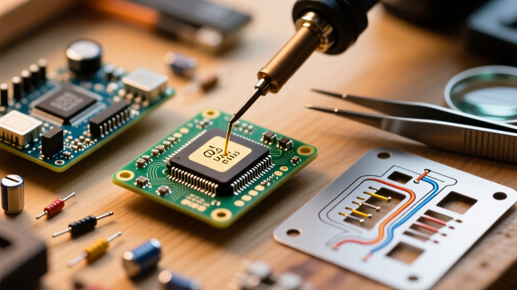
According to our stencil specialist, the central thermal pad of a QFN is the primary culprit behind solder voiding and component floating. If you apply a 1:1 aperture ratio for the thermal pad, the volume of solder paste will trap flux vapors during the reflow phase.
Calculating the Reduction
The industry standard is to reduce the thermal pad aperture area by 10% to 20% and divide it into a 'window-pane' or cross-hatch pattern. For example, if your QFN has a 5mm x 5mm thermal pad:
- Total Pad Area: 25mm²
- Target Reduction (15%): 3.75mm² reduction, leaving 21.25mm² of solder coverage.
- Execution: Divide the pad into four smaller squares (or a 3x3 grid for larger pads) with a 0.5mm to 1.0mm keep-out channel between them. This creates escape routes for outgassing flux.
For the perimeter leads, a 1:1 ratio is generally acceptable for 0.5mm pitch, but for 0.4mm pitch, experts recommend a 10% width reduction to prevent solder bridging, which remains the most common defect in fine-pitch advanced solder paste applications.
Hand-Rework vs. Automated Reflow: A Process Engineer's View
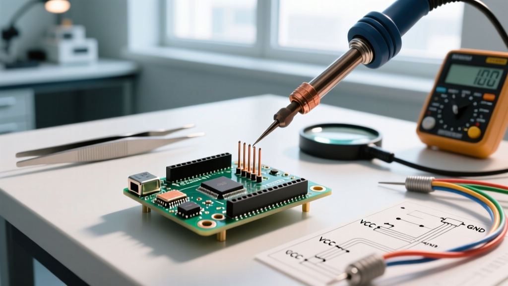
While automated reflow ovens with multi-zone profiling are ideal for volume production, prototyping and repair require manual hot-air rework. Our aerospace rework technician outlined a bulletproof, step-by-step methodology for hand-soldering a QFN using a bottom preheater and a top-air station.
- Board Preparation: Clean the PCB pads with 99% isopropyl alcohol (IPA). Apply a microscopic layer of Amtech NC-559-V2-TF tack flux to the pads. The tackiness is crucial for aligning the QFN without it shifting when air hits it.
- Preheating: Set your IR or ceramic preheater to 120°C - 130°C. This brings the entire PCB assembly close to the solder paste's liquidus threshold, drastically reducing the amount of localized hot air needed later.
- Component Placement: Using fine-point tweezers or a vacuum pen, align the QFN. The tack flux will hold it securely. Verify alignment under a stereo microscope; even a 0.1mm misalignment on a 0.4mm pitch will cause bridging.
- Top-Down Reflow: Set your hot air station (e.g., Quick 861DW) to 320°C with a low airflow setting (approx. 30-40%). Use a nozzle that encompasses the entire QFN body. Apply heat evenly in a circular motion from a height of 15mm.
- The 'Settle' Indicator: Watch closely. As the solder paste reaches its liquidus state (approx. 217°C for SAC305), surface tension will pull the component into perfect alignment. You will see the QFN physically 'drop' or settle by a fraction of a millimeter. Once this happens, remove the heat immediately to prevent pad lifting.
Inspection: Catching Head-in-Pillow and Voiding
Because QFN leads are hidden beneath the component body, standard visual inspection is insufficient. Our experts emphasize two critical failure modes that must be checked against IPC-A-610 acceptability standards.
1. Head-in-Pillow (HiP) Defects
HiP occurs when the solder paste on the PCB pad and the solder pre-coat on the QFN lead melt but fail to coalesce, leaving a microscopic gap. This is usually caused by insufficient heat reaching the inner rows of the QFN, or by PCB warping during the reflow cycle. Using a bottom preheater mitigates warping and ensures the inner leads reach the required thermal mass.
2. Thermal Pad Voiding
Solder voids in the thermal pad reduce heat dissipation and mechanical strength. According to NASA and IPC reliability guidelines, voiding should generally not exceed 25% of the total pad area for Class 2 assemblies, and many high-reliability OEMs demand less than 15%. Without an X-ray machine, hobbyists can sometimes infer severe voiding by observing excessive solder squeeze-out on the perimeter, indicating that vapor pressure forced the solder outward instead of settling under the pad.
FAQ: QFN Soldering Troubleshooting
Why is my QFN floating or tilting after reflow?
Component floating is almost always caused by excessive solder volume on the central thermal pad. When the paste melts, trapped flux vapors expand. If the stencil aperture wasn't reduced or window-paned, the vapor pressure acts like a hovercraft, lifting the IC. Once the vapor escapes, the IC drops unevenly, causing open circuits on one side. Reduce your thermal pad stencil aperture by 15% and ensure your reflow profile has an adequate soak zone (60-90 seconds at 150°C-175°C) to allow volatiles to burn off before liquidus.
Can I use Type 3 solder paste for a 0.4mm pitch QFN?
Technically, you can attempt it, but experts strongly advise against it. Type 3 paste has larger solder spheres (mesh -200/+325). When deposited through a 3-mil stencil on tiny 0.4mm pads, the large spheres cause 'gaping' and inconsistent deposition, leading to insufficient solder joints or bridging. Always step up to Type 4 for 0.5mm pitch, and Type 5 or Type 6 for 0.4mm and 0.3mm pitch QFNs to ensure smooth paste release and uniform reflow.
Is liquid flux better than tack flux for QFN rework?
For initial SMT stencil printing, liquid or standard gel fluxes inside the solder paste are standard. However, for manual hand-rework, tack flux (like Amtech NC-559) is vastly superior. Liquid flux will boil and cause the lightweight QFN to skate across the board when hit with hot air. Tack flux provides the necessary mechanical adhesion to keep the component anchored while providing the chemical cleaning action required for a reliable intermetallic bond.