
From Laboratory Curiosity to PCB Assembly Staple
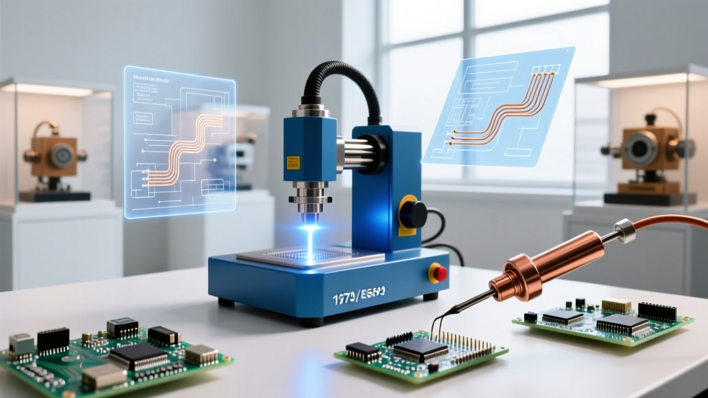
The trajectory of the laser soldering machine from a niche laboratory experiment to a cornerstone of high-reliability printed circuit board (PCB) assembly is a masterclass in applied photonics. Unlike traditional contact methods like wave soldering or selective iron-based systems, modern laser systems deliver non-contact, highly localized thermal energy. This capability is no longer a luxury; in 2026, it is an absolute requirement for assembling dense microelectronics, automotive power modules, and fragile RF components. To understand where the technology is going, buyers and engineers must understand the physical limitations that drove its historical evolution.
The 1970s and 1980s: The CO2 and Nd:YAG False Starts
The earliest attempts at using photons for solder reflow occurred in the late 1970s, utilizing Carbon Dioxide (CO2) lasers operating at a 10.6 µm wavelength. The fundamental physics of this era doomed the technology for mainstream electronics. Copper and gold—the primary conductive materials in PCBs—are highly reflective to far-infrared light. Instead of heating the solder joint, the CO2 laser beam would either scatter dangerously or be aggressively absorbed by the FR4 fiberglass substrate, resulting in charred boards and delaminated copper traces.
By the mid-1980s, engineers pivoted to Nd:YAG lasers (1064 nm). While the near-infrared (NIR) wavelength offered better absorption in standard tin-lead (Sn63/Pb37) solder alloys, it still struggled immensely with pure copper heat sinks and gold-plated RF pads. The Fraunhofer Institute for Laser Technology ILT and similar research bodies documented how the high reflectivity of copper at 1064 nm required massive, uncontrolled power spikes to initiate melting, often leading to severe thermal shock and component destruction.
The 1990s Diode Laser Breakthrough
The true commercial viability of the laser soldering machine began in the 1990s with the maturation of high-power semiconductor diode lasers operating in the 808 nm to 980 nm range. This wavelength shift was revolutionary. Solder alloys, particularly the emerging lead-free variants like SAC305 (Sn96.5/Ag3.0/Cu0.5), exhibit vastly superior absorption rates in the 900+ nm spectrum compared to the base copper substrate.
This differential absorption allowed the laser to heat the solder paste or preform rapidly while the copper pad acted as a natural thermal buffer, preventing substrate damage. Pioneering companies like Japan Unix and PacTech introduced the first automated inline diode laser systems. These early machines utilized basic galvanometer scanners to position the beam, replacing the slow, mechanical movement of a physical soldering iron tip and reducing cycle times per joint from 3 seconds down to under 0.5 seconds.
Modern Era: Blue Diode and Fiber Lasers (2020s to Present)
As the electronics industry shifted toward electric vehicles (EVs), renewable energy inverters, and 5G infrastructure, the physical demands on solder joints changed. Power electronics now rely on Silicon Carbide (SiC) and Gallium Nitride (GaN) semiconductors, which require massive copper busbars and thick-ground planes to dissipate extreme heat loads. Near-infrared diode lasers were once again bottlenecked by copper's reflectivity.
The introduction of high-power blue diode lasers (450 nm) by companies like Laserline GmbH and NUBURU completely disrupted the market. At 450 nm, copper's absorption rate jumps from less than 5% (in the NIR spectrum) to over 60%. This allows modern laser soldering machines to reflow large-volume solder preforms on thick copper power modules in seconds, without the need for aggressive, board-damaging pre-heating profiles. Simultaneously, single-mode fiber lasers (1070 nm) with advanced beam-shaping optics (like spiral or ring-core profiles) have become the standard for ultra-precise micro-soldering in medical devices and wearables, where joint tolerances are measured in microns.
Technical Comparison Matrix: Laser Soldering Wavelengths
| Laser Type | Wavelength | Copper Absorption | Primary Use Case | Approx. System Cost (2026) |
|---|---|---|---|---|
| NIR Diode | 808 - 980 nm | ~5% - 10% | Standard PCB assembly, wire-to-board, flexible circuits | $35,000 - $65,000 |
| Blue Diode | 440 - 460 nm | ~60% - 65% | EV power modules, thick copper busbars, SiC/GaN packages | $120,000 - $250,000+ |
| Fiber (Single Mode) | 1064 - 1080 nm | ~8% - 12% | Microelectronics, medical sensors, 01005 passives | $80,000 - $140,000 |
| UV Laser | 355 nm | High (Metals/Polymers) | Clean ablation, selective solder mask removal, niche micro-joints | $150,000+ |
Critical Failure Modes and Edge Cases
Buying a laser soldering machine without understanding its failure modes is a fast track to scrapped batches and low yields. As outlined by the IPC (Association Connecting Electronics Industries) standards for advanced assembly, non-contact thermal processes introduce unique edge cases:
- MLCC Thermal Shock Cracking: Multi-Layer Ceramic Capacitors (MLCCs) are highly susceptible to steep thermal gradients. If a laser beam dwells too long on one side of an MLCC pad without symmetrical beam-splitting, the resulting asymmetric expansion will crack the ceramic dielectric, leading to latent field failures. Modern systems mitigate this using 'bifocal' or 'ring' beam profiles that heat both pads simultaneously.
- Flux Outgassing and Pyrometer Blinding: Closed-loop temperature control relies on inline pyrometers reading the joint's infrared emission. When no-clean or water-soluble fluxes activate, they outgas violently. This flux plume can scatter the pyrometer's sensor beam, causing the system to falsely read a low temperature and pump excessive laser power into the joint, resulting in solder boil and splatter.
- The Tombstone Effect in Passives: In 0201 and 01005 chip components, if the laser's spatial intensity profile is not perfectly calibrated, one pad will reach reflow temperature milliseconds before the other. The surface tension of the molten solder on the heated side will pull the component upright, creating a 'tombstone' defect.
Buyer's Framework: ROI and Capital Expenditure
When evaluating the integration of a laser soldering machine into a production line in 2026, the capital expenditure (CapEx) must be weighed against throughput and yield metrics. A high-end 5-axis automated blue laser cell from integrators like PacTech or Finetech can easily exceed $180,000. However, for automotive Tier 1 suppliers, the ROI is typically realized within 14 to 18 months.
"The shift to blue laser technology for power electronics isn't just about speed; it's about achieving void-free solder joints in high-thermal-mass assemblies that selective wave soldering simply cannot touch without destroying temperature-sensitive silicon."
For low-to-medium volume contract manufacturers (CMs), a desktop NIR diode laser rework station (priced between $25,000 and $45,000) offers a compelling alternative to manual micro-soldering. These systems drastically reduce operator fatigue, eliminate tip-wear consumables, and provide traceable thermal profiles for every single joint—a critical requirement for aerospace and medical device compliance.
Conclusion
The evolution of the laser soldering machine is a direct reflection of the electronics industry's relentless push toward miniaturization and higher power densities. From the destructive CO2 experiments of the 1970s to the precision blue diode systems assembling next-generation EV inverters today, laser soldering has matured from a theoretical alternative into an indispensable manufacturing technology. For modern electronics manufacturers, selecting the correct wavelength, beam profile, and closed-loop monitoring system is no longer optional—it is the defining factor in product reliability and production yield.