
The Component-Sensitivity Matrix: A Decision Framework for Soldering Electrical Components
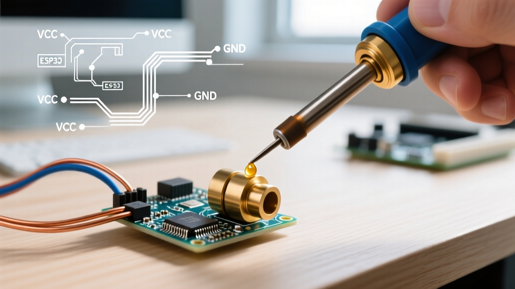
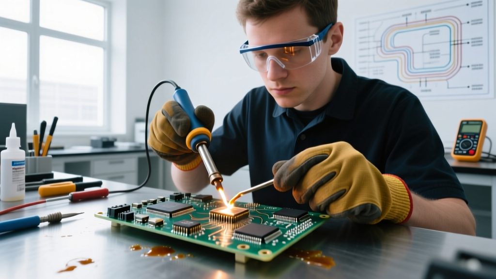
Soldering electrical components is not a monolithic skill; it is a series of thermodynamic decisions. Applying the same 400°C chisel tip to a 10 AWG XT60 battery connector and a 0402 SMD multilayer ceramic capacitor (MLCC) will yield catastrophic results—either a cold, high-resistance joint on the wire or a micro-fractured, shorted capacitor. To achieve IPC-compliant reliability, engineers and technicians must adopt a structured decision framework. This guide provides a rigorous, step-by-step methodology for selecting the optimal alloy, heat delivery system, tip geometry, and flux chemistry based on the specific thermal mass and sensitivity of your target components.
Table 1: Component Thermal Mass & Sensitivity Matrix
| Component Type | Thermal Mass | Max Temp / Dwell Limit | Recommended Tip Geometry | Ideal Alloy Profile |
|---|---|---|---|---|
| 0402 / 0603 SMD Passives | Extremely Low | 260°C / 2-3 seconds | Micro-Conical (0.4mm) | Sn42/Bi57 (Low Temp) |
| QFP / SOIC Integrated Circuits | Low to Medium | 300°C / 3-5 seconds per pin | Knife (2.5mm) or MiniWave | Sn63/Pb37 or SAC305 |
| Through-Hole Electrolytic Caps | Medium | 350°C / 4 seconds | Chisel (2.4mm - 3.2mm) | Sn60/Pb40 (Rosin Core) |
| Heavy Gauge Wire (10-12 AWG) | Very High | 400°C+ / Until wetting occurs | Heavy Chisel / Spade (5mm+) | Sn63/Pb37 (Thick Core) |
Step 1: Classify the Component and Select the Alloy
The first branch of the decision tree requires identifying the thermal limits of the electrical components you are soldering. The melting point and plastic state of your solder alloy dictate your baseline iron temperature.
Leaded vs. Lead-Free vs. Low-Temperature Alloys
- Sn63/Pb37 (Eutectic Leaded): Melts at exactly 183°C. This remains the gold standard for hobbyist, prototyping, and aerospace repair work due to its sharp eutectic transition (no plastic phase) and superior wetting characteristics. Set your station to 300°C - 330°C for standard through-hole work.
- SAC305 (Lead-Free): Composed of 96.5% Tin, 3.0% Silver, and 0.5% Copper. Melts at 217°C. Mandatory for commercial RoHS-compliant manufacturing. Requires higher iron temperatures (350°C - 380°C) and more aggressive flux activators to overcome the sluggish wetting inherent to lead-free alloys.
- Sn42/Bi57 (Bismuth Low-Temp): Melts at 138°C. This is your decision-framework override for highly sensitive RF modules, flexible PCBs, or components already subjected to one reflow cycle. It prevents pad lifting but is mechanically brittle; it must never be used on high-vibration connectors.
Step 2: Heat Delivery System Selection
When soldering electrical components with varying thermal masses, the speed of thermal recovery is more critical than raw wattage. A 75W iron with poor thermal coupling will fail where a 40W iron with advanced cartridge technology succeeds.
Station Comparison: Conduction vs. Integrated Cartridge
For high-density PCB rework, the market is dominated by two distinct architectures:
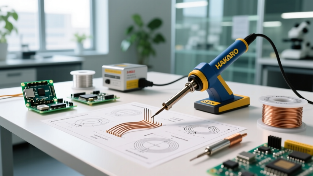
- Hakko FX-951 (Approx. $350): Utilizes the T18 tip series where the heating element is inserted into the back of the tip. Thermal transfer relies on physical contact between the ceramic heater and the tip's inner cavity. Recovery time from a 350°C drop takes roughly 6 to 8 seconds. Excellent for general through-hole and mid-sized SMD work.
- JBC CD-2BE (Approx. $680): Uses the C245 cartridge system where the heater and sensor are integrated directly into the tip's copper core. This eliminates the air gap, allowing the tip to reach 350°C in under 2 seconds and recover from heavy ground-plane heat sinks almost instantaneously. This is the mandatory choice for soldering complex electrical components like BGA pads or multi-layer ground vias.
- Pine64 Pinecil V2 (Approx. $45): A PD-powered portable iron using T12-compatible tips. While exceptional for field repairs and basic wiring, its thermal mass limits make it unsuitable for sustained soldering of heavy electrical components or large copper pours.
Step 3: Tip Geometry Decision Tree
According to NASA-STD-8739.3 workmanship requirements, the tip must transfer heat efficiently without bridging adjacent conductors. Select your geometry based on the pad shape, not just personal preference.
Expert Rule of Thumb: The width of the chisel or bevel tip should match the width of the pad or the diameter of the wire being soldered. Using a tip that is too small causes dwell-time overruns; using a tip that is too large risks melting adjacent component housings.
- Knife Tips (e.g., JBC C245-903): The edge is used for precision SMD work and drag-soldering QFP integrated circuits. The flat side can be used for tinning ground planes.
- Chisel Tips (e.g., Hakko T18-D24): The standard for through-hole components and 0.1" header pins. The flat face maximizes surface area contact with cylindrical leads.
- Conical / Pencil Tips: Generally discouraged for heavy thermal work due to minimal surface area contact, but necessary for 0201 and 0402 micro-passives where pad clearance is under 0.2mm.
Step 4: Flux Chemistry and Cleaning Protocol
Flux removes metal oxides, enabling the metallurgical bond. The IPC standards dictate that flux selection must align with the end-use environment of the PCB. When soldering electrical components in high-impedance analog circuits, flux residue can cause parasitic leakage currents.
Flux Selection Matrix
- No-Clean (e.g., Kester 951): Leaves a minimal, non-conductive, and non-corrosive residue. Ideal for RF boards and high-density digital logic where washing is impractical.
- Rosin Mildly Activated - RMA (e.g., Kester 44): The standard rosin-core wire solder. Provides excellent wetting for general electrical wiring and through-hole components. Residue is benign but sticky, attracting dust over time.
- Tacky / Gel Flux (e.g., Amtech TAC-01): Syringe-dispensed, highly viscous flux. Mandatory for SMD drag soldering and BGA reballing. It holds components in place via surface tension while providing sustained oxide removal over long heat cycles.
- Water-Soluble (e.g., Kester 331): Highly aggressive organic acids. Used for heavily oxidized wires or difficult-to-solder metals (like nickel). Warning: Must be thoroughly cleaned with DI water post-soldering, or it will cause severe galvanic corrosion and dendrite growth.
Failure Mode Analysis: When the Framework Fails
Even with the correct parameters, soldering electrical components can yield defects if execution falters. Recognizing these failure modes is critical for troubleshooting.
1. Tombstoning (SMD Passives)
The Defect: One end of a capacitor lifts off the pad, standing upright like a tombstone.
The Cause: Uneven heating. If the iron tip contacts one pad before the other, or if one pad is connected to a ground plane (acting as a heat sink) while the other is a thin signal trace, the solder on the hotter pad melts first. The surface tension of the liquid solder pulls the component upright.
The Fix: Pre-heat the board to 100°C using a hot air gun or PCB preheater to equalize the thermal delta between the pads before applying the iron.
2. Pad Lift and Delamination
The Defect: The copper trace separates from the FR4 fiberglass substrate.
The Cause: Excessive dwell time. The IPC J-STD-001 standard generally limits hand-soldering dwell time to 3-4 seconds per joint. Prolonged heat degrades the epoxy resin binding the copper to the board.
The Fix: If a joint isn't flowing within 3 seconds, remove the iron. Let the board cool completely, apply fresh liquid flux, and attempt again with a larger tip or higher temperature, rather than holding a small tip against the pad indefinitely.
3. Disturbed Joints (Frosted Appearance)
The Defect: The solder joint looks grainy, dull, and crystalline, lacking a smooth concave fillet.
The Cause: Micro-movements during the phase transition from liquid to solid. In non-eutectic lead-free alloys (like SAC305), there is a 'plastic' phase where the solder is semi-solid. Moving the component during this phase fractures the crystalline matrix.
The Fix: Use a mechanical jig or third-hand tool to hold the wire or component absolutely rigid until the solder has fully crystallized and cooled below 150°C.
Final Verdict: Building Your Soldering Arsenal
Soldering electrical components flawlessly requires abandoning the 'one iron, one wire' mentality. By systematically classifying your component's thermal mass, selecting an alloy that matches the thermal budget, and deploying the correct tip geometry and flux chemistry, you transition from guesswork to engineered reliability. For a professional bench in 2026, investing in a JBC cartridge-based station for SMD micro-work, paired with a heavy-duty Hakko for thick-gauge wiring, and stocking both Sn63/Pb37 and SAC305 alloys, will cover 99% of all electronic assembly scenarios you will encounter.