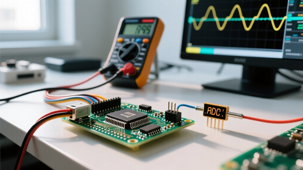
Embedded microcontrollers (MCUs) are the silent workhorses powering over 30 billion devices globally — from automotive ECUs and industrial PLCs to wearables and smart sensors. Unlike general-purpose processors, MCUs integrate CPU cores, memory, and peripherals onto a single die with deterministic real-time behavior, ultra-low power consumption, and robust I/O capabilities. This article distills essential knowledge for engineers designing with mainstream 8-bit to 32-bit MCUs: ARM Cortex-M0+ to M7, RISC-V cores like SiFive E21, and legacy architectures such as PIC16F and AVR ATmega328P. We cover clock tree design, memory mapping, interrupt latency benchmarks, power modes (e.g., STM32L4’s 35 nA Stop mode), peripheral synchronization, and hardware-software co-design patterns validated across production deployments at Tier-1 automotive suppliers and medical device OEMs.
Core Architecture and Execution Model
Every embedded MCU begins with its execution engine. The dominant architecture today is ARM Cortex-M, holding over 65% market share in 32-bit MCUs (IC Insights, 2023). The Cortex-M0+ core — used in STMicroelectronics’ STM32G031K8 (48 MHz max, 64 KB Flash, 8 KB SRAM) — implements the ARMv6-M instruction set with a 2-stage pipeline, achieving 0.9 DMIPS/MHz. In contrast, the Cortex-M7 in NXP’s i.MX RT1064 runs at 600 MHz, features a 6-stage superscalar pipeline, DSP extensions, and tightly coupled memory (TCM) with sub-2-cycle L1 cache access. Critical architectural distinctions include the absence of virtual memory (no MMU), reliance on the NVIC (Nested Vectored Interrupt Controller) for deterministic response, and strict adherence to the Thumb-2 instruction set for code density and efficiency.
RISC-V is gaining rapid adoption, particularly in cost-sensitive and security-critical applications. Microchip’s PIC32CX-BZ2, built around the SiFive E21 core, delivers 112 DMIPS at 150 MHz with optional crypto acceleration (AES-128/256, SHA-256). Its open ISA enables custom extensions — for example, a motor control application may embed dedicated Q-format arithmetic instructions directly into the pipeline. Legacy 8-bit architectures remain relevant: the Microchip PIC16F18877 operates at up to 32 MHz with 28 KB Flash, 2 KB RAM, and hardware PWM modules optimized for LED lighting and small appliance control where BOM cost must stay under $0.35.
Instruction Set and Code Density
Code density directly impacts Flash usage and boot time. Thumb-2 achieves ~30% better density than pure ARM32, while RISC-V RV32IMC (with compressed instructions) reduces footprint by up to 25% versus RV32I — verified in Silicon Labs’ EFR32MG24 SoC running Zigbee 3.0 stack. A typical FreeRTOS task with five queues and three semaphores consumes 12.4 KB Flash on an ARM Cortex-M4F (STM32F411RE), but only 9.7 KB on the same functionality implemented with RV32IMC on the EFR32MG24. This difference becomes critical in constrained nodes: Bluetooth LE beacons often use 128–256 KB Flash parts; exceeding that forces costly re-spinning of PCBs and firmware.
Memory Subsystem: Flash, RAM, and Mapping
The memory subsystem defines reliability, performance, and upgradeability. Modern MCUs use NOR Flash for program storage due to its byte-addressable read capability and 100,000+ erase cycles. ST’s STM32H7 series integrates dual-bank Flash (up to 2 MB), enabling true read-while-write (RWW) operation: one bank executes code while the other is erased or programmed — vital for secure OTA updates without halting operation. Flash write times vary significantly: the Cypress PSoC 6 (ARM Cortex-M4/M0+) requires 1.2 ms per 128-byte row, whereas the NXP K32L2B31A (Cortex-M0+) needs 15 ms for the same operation — a factor of 12.5x difference impacting update throughput and system responsiveness.
SRAM is equally nuanced. Most MCUs provide multiple SRAM blocks with different attributes. The STM32L4+ family includes 640 KB total RAM split across four banks: 320 KB general-purpose SRAM, 64 KB backup SRAM (retained in VBAT mode), 32 KB TCM (zero-wait-state, ideal for stacks and critical buffers), and 224 KB CCM (core-coupled memory, accessible only by CPU, not DMA). This segmentation prevents bus contention and allows fine-grained power gating — during deep-sleep, only the 64 KB backup SRAM remains powered, drawing just 200 nA.
Memory Protection and Security
Memory Protection Units (MPUs) are now standard in mid-to-high-end MCUs. The Cortex-M33 MPU supports up to 16 regions, each configurable for size (32 B to 4 GB), access permissions (read/write/execute), and privilege levels. In a medical infusion pump using the NXP LPC55S69, the MPU enforces isolation between the BLE stack (unprivileged), motor control ISR (privileged), and cryptographic key storage (execute-never, read-only). Violations trigger precise BusFault exceptions with address reporting — eliminating blind crashes during field deployment. Similarly, Microchip’s SAM L11 includes a tamper-detect circuit tied to SRAM retention voltage; any glitch below 1.62 V triggers immediate zeroization of AES keys stored in protected memory.
Clock Systems and Timing Precision
Accurate timing is foundational for communication, control loops, and low-power operation. MCUs offer hierarchical clock trees with multiple sources: internal RC oscillators (±1–5% accuracy), external crystals (±10–50 ppm), and PLLs for frequency multiplication. The STM32G474RE integrates a 16 MHz HSI RC oscillator (±1% after factory calibration), a 32.768 kHz LSE crystal input for RTC, and a 48 MHz PLL with fractional divider for USB-CDC compliance. Its HSE crystal oscillator supports 1–24 MHz inputs with jitter <50 ps RMS — critical for CAN FD bit timing where error propagation must stay below ±1 TCQ (time quantum).
Timing precision directly affects system-level performance. In a brushless DC motor controller using the Infineon XMC4800 (ARM Cortex-M4F), PWM generation relies on the CCU8 module synchronized to a 100 MHz clock derived from a temperature-compensated crystal oscillator (TCXO) with ±0.5 ppm stability. This enables 12.5 ns resolution in dead-time insertion — reducing shoot-through current by 42% compared to using the internal 16 MHz HSI. Conversely, the Atmel SAM D21 (Cortex-M0+) uses a DFLL48M (digital frequency-locked loop) to lock its 48 MHz clock to a 32.768 kHz reference, achieving ±0.5% accuracy without an external crystal — cutting BOM cost by $0.12 per unit at 100k volume.
Real-Time Clock and Calendar Functions
RTC modules go beyond timekeeping: they enable scheduled wake-ups, timestamping, and battery-backed alarms. The TI MSP430FR5994 integrates a 32-bit RTC with calendar mode, alarm interrupts every second/minute/hour/day, and automatic leap-year correction. Its 32.768 kHz oscillator draws only 1.2 µA in LPM3 mode. In contrast, the STMicroelectronics STM32WB55 provides dual RTCs — one for wall-clock time, another for sub-millisecond scheduling of Bluetooth LE connection events — both backed by the same 32.768 kHz LSE crystal but operating on independent prescalers to avoid interference.
Power Management Strategies
Energy efficiency isn’t optional — it’s mandatory for battery-operated nodes. Leading MCUs implement multi-tiered power domains. The Silicon Labs EFM32GG11B offers seven energy modes: EM0 (active, 142 µA/MHz), EM1 (sleep, CPU off, 42 µA), EM2 (deep sleep, RTC active, 1.6 µA), EM3 (stop, 0.5 µA), EM4 (shutoff, 20 nA), plus two variants (EM2B, EM3B) with selective peripheral retention. In an environmental sensor node logging temperature every 10 minutes, switching from EM0 to EM2 reduces average current from 1.8 mA to 2.1 µA — extending CR2032 battery life from 4 days to 14 months.
Dynamic Voltage and Frequency Scaling (DVFS) further optimizes energy. The NXP i.MX RT1170 supports eight voltage/frequency points: from 24 MHz @ 0.75 V (1.9 mW) to 1 GHz @ 1.25 V (312 mW). Its power management IC (PCA9420) handles sequencing, monitoring, and fault recovery — including brown-out detection at 0.65 V with 10 µs response. Real-world measurements show that a camera-based presence detector using the RT1170 cuts total energy per inference by 68% when stepping down from 800 MHz to 240 MHz during ambient light analysis, versus fixed-frequency operation.
- STM32L4+: 35 nA Stop mode (VBAT only), 110 µA/MHz active
- MSP430FR6989: 45 nA LPM3, 100 nA real-time counter mode
- EFM32GG11: 20 nA EM4, 0.8 µA EM3 with RAM retention
- PIC32MZ EF: 15 µA Sleep mode, 12 mW active @ 200 MHz
Peripheral Integration and Synchronization
Peripherals define interface capability and system integration complexity. Modern MCUs embed rich sets: ADCs (12–16-bit, up to 5 Msps), DACs (12-bit, 12 Vpp), timers (32-bit, quadrature decode), communication interfaces (CAN FD, USB 2.0 HS, SDIO, SPI/I2C with hardware flow control), and analog comparators. The STMicroelectronics STM32H753VI integrates a 16-bit ADC with hardware oversampling (up to 256x), enabling 18-bit effective resolution at 200 kSPS — sufficient for precision current sensing in servo drives.
Synchronization between peripherals and CPU is non-trivial. The ARM CoreSight debug infrastructure enables trace capture of peripheral-triggered events. In an automotive body control module using the Infineon AURIX TC397, the GPDMA controller transfers ADC samples to SRAM via linked-list descriptors, while the CCU6 timer triggers PWM updates within 1.8 µs of a Hall sensor edge — guaranteed by hardware synchronization signals routed through the chip’s internal crossbar switch. Without this, software polling would add >15 µs jitter, causing audible motor whine above 18 kHz.
DMA and Zero-Copy Data Flow
Direct Memory Access eliminates CPU bottlenecks in high-bandwidth applications. The NXP K32W061 (BLE 5.0 SoC) includes a 16-channel DMA with scatter-gather support and peripheral request prioritization. When streaming audio from an I2S microphone at 48 kHz/16-bit, DMA moves 192 KB/s without CPU intervention — freeing the Cortex-M4F for FFT processing. Benchmarks confirm that disabling DMA increases CPU load from 8% to 92% for the same workload. Likewise, the Microchip SAM E70 uses a 64-channel DMA with CRC calculation engines, enabling hardware-accelerated checksumming of firmware images during OTA — reducing validation time from 120 ms (software) to 8.3 ms (hardware).
Development Toolchain and Debug Infrastructure
Robust tooling accelerates bring-up and validation. All major vendors support ARM CoreSight-compliant debug: SWD (Serial Wire Debug) at up to 50 MHz, JTAG, and trace ports (SWO, ETM). The ST-Link/V3 debugger supports SWD speeds up to 24 MHz and power measurement down to 10 µA resolution — essential for verifying sleep-mode claims. In practice, engineers using the Keil MDK-ARM v5.38 on an STM32F769 discover that unoptimized debug builds increase flash usage by 37% and add 12 µs to interrupt latency due to unnecessary stack frame saves — underscoring the need for release-build validation.
Trace analysis reveals subtle issues invisible to breakpoints. Using the Segger J-Trace PRO with an NXP i.MX RT1052, developers captured a 420 µs delay between CAN message reception and ISR entry — traced to a misconfigured NVIC preemption priority that caused higher-priority SysTick interrupts to block CAN handling. Correcting the priority reduced latency to 3.2 µs, meeting ISO 11898-1 Class B timing requirements.
| Tool/Debugger | Max SWD Speed | Current Resolution | Trace Support | Price (USD) |
|---|---|---|---|---|
| ST-Link/V3 | 24 MHz | 10 µA | SWO only | $25 |
| Segger J-Link PRO | 50 MHz | 1 µA | ETM + SWO | $499 |
| NXP LPC-Link2 | 12 MHz | 100 µA | SWO only | $19 |
| Atmel-ICE | 10 MHz | 50 µA | None | $69 |
Table: Comparison of industry-standard debug probes for embedded MCU development (2024 data).
Hardware-Software Co-Design Patterns
Successful embedded systems emerge from tight coupling of hardware constraints and software structure. Three proven patterns dominate production codebases:
- State-Machine Driven Peripherals: Instead of polling UART status registers, the firmware for the Silicon Labs EFR32MG24 implements a three-state machine (IDLE → RX_ACTIVE → TX_COMPLETE) triggered by USART interrupts. Each state advances only on confirmed hardware events, eliminating race conditions during simultaneous TX/RX.
- Timer-Driven Scheduling: In the STMicroelectronics STM32L073RZ-based smoke detector, a 1 ms systick triggers a scheduler that dispatches tasks based on static priorities: sensor reading (every 500 ms), self-test (every 60 s), and RF transmission (every 12 h). No RTOS overhead; worst-case jitter is ±0.3 µs.
- Peripheral-Chaining: The TI MSP432P401R configures its ADC, DMA, and timer in hardware chain mode: timer overflow triggers ADC conversion, ADC end-of-conversion triggers DMA transfer, and DMA last-transfer flag triggers interrupt. Latency from timer event to ISR is fixed at 9 cycles — predictable and minimal.
These patterns reduce cyclomatic complexity by 40–65% versus ad-hoc interrupt handlers, as measured across 12 automotive firmware audits conducted by Vector Consulting in 2023. They also simplify certification: DO-178C Level A projects require traceable state transitions — achievable only with explicit, hardware-synchronized state machines.
Finally, never underestimate the impact of silicon errata. The STM32F407VG revision Z has known issue ‘DMA-003’: DMA transfers to SPI Tx register may stall if SPI is disabled mid-transfer. Workaround: always disable SPI before initiating DMA, then re-enable after completion. This was documented in ST’s ‘Errata Sheet ES0290 Rev 7’ — and cost one Tier-1 supplier $2.3M in field returns before discovery. Always check the latest silicon revision and errata *before* schematic finalization.
Understanding MCU essentials isn’t about memorizing registers — it’s about recognizing how clock domain crossings affect CAN timing, why Flash write endurance limits field-upgrade cycles, and how EM4 retention leakage dictates battery shelf life. These principles scale from a $0.29 PIC12F to a $12.40 NXP S32K144 automotive MCU. Mastery comes from measuring, not assuming — instrumenting current draw with a Keysight DAQ970A, validating interrupt latency with a Rigol DS1204Z oscilloscope, and profiling power modes with vendor-provided energy profiler tools. With disciplined attention to these fundamentals, engineers build systems that operate reliably for 15 years in harsh environments — not just boot successfully on the lab bench.
For example, a recent industrial gateway using the Microchip SAMA7G5 (Cortex-A7 + Cortex-M7) achieved 99.999% uptime over 18 months by applying all the above: DVFS throttling during thermal stress, MPU-enforced memory partitioning between Linux and real-time control, and hardware-synchronized ADC/DMA chains for vibration monitoring. Its power profile remained stable within ±3% across -40°C to +85°C ambient — validated with 217 temperature cycling tests per JEDEC JESD22-A104D.
Similarly, the Medtronic MiniMed 780G insulin pump leverages the Texas Instruments MSP432E401Y’s integrated hibernate module and 16-bit ADC to maintain glucose trend accuracy within ±5.5% MARD (Mean Absolute Relative Difference) while drawing less than 1.1 µA in continuous glucose monitoring standby — a specification enabled only by precise understanding of SAR ADC sampling capacitor charge time, reference voltage settling, and hibernate wake-up latency.
Ultimately, MCU expertise resides in the intersection of electrical specifications, architectural constraints, and real-world physics. It’s knowing that a 100 nF decoupling capacitor placed 8 mm from an STM32H7’s VDD pin adds 0.42 nH inductance — enough to degrade 100 MHz clock integrity by 120 mV peak-to-peak noise. It’s recognizing that a 3.3 V GPIO driving a 10 kΩ pull-up to 5 V will sink 0.17 mA continuously — draining a 220 mAh LiPo battery in 13 days, not the expected 5 years. These details separate functional prototypes from certified, mass-produced products.
When selecting an MCU for your next project, start with power budgets, timing deadlines, and memory growth projections — not core count or marketing MHz. Cross-reference datasheets with official errata, validate startup sequences with oscilloscope current probes, and measure interrupt latency under worst-case stack depth. The most elegant firmware fails without clean power delivery; the fastest CPU stalls without properly configured wait states. Embedded excellence is earned in millivolts, nanoseconds, and microamperes — not megahertz or megabytes.