
Decoding the Arduino Uno Circuit Schematic for Custom Hardware
When transitioning from a breadboard prototype to a finalized printed circuit board (PCB), hardware engineers and advanced makers frequently consult the official Arduino Uno circuit schematic. While the off-the-shelf development board is unparalleled for rapid prototyping, embedding the entire Uno design into a custom product is rarely the optimal engineering choice. This project suitability analysis dissects the classic Arduino Uno R3 schematic, evaluating its power delivery network, microcontroller architecture, and peripheral circuits to determine when you should replicate it, when you should strip it down, and when you should abandon it entirely for a barebones ATmega328P implementation.
Core Architecture Breakdown: What Are You Actually Copying?
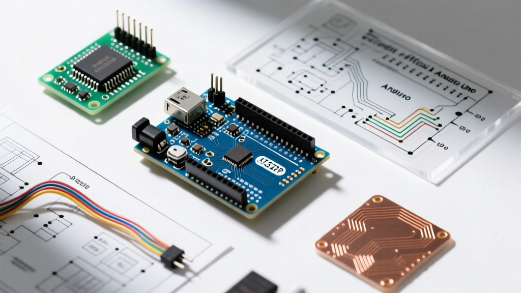
The standard Arduino Uno R3 documentation reveals a dual-microcontroller architecture. The primary brain is the ATmega328P-PU (or AU in SMD variants), an 8-bit AVR microcontroller operating at 16MHz. However, the schematic also includes a secondary microcontroller: the ATmega16U2-MU, which handles USB-to-Serial conversion. Additionally, the board features an NCP1117 linear voltage regulator, a 16MHz ABLS crystal oscillator, and an array of status LEDs and protection diodes.
Understanding this division of labor is critical for project suitability. If your end product requires direct USB communication without an external FTDI programmer, retaining the ATmega16U2 circuit from the schematic is mandatory. If your device will be programmed once via an In-Circuit Serial Programmer (ICSP) and deployed in the field, the 16U2 and its associated USB-B connector represent dead weight, consuming valuable PCB real estate and adding unnecessary quiescent current draw.
Power Delivery Network (PDN) Analysis: The Linear Regulator Bottleneck
One of the most heavily debated aspects of the Arduino Uno circuit schematic is its power delivery network. The board utilizes an NCP1117ST50T3G, a 5V linear dropout (LDO) regulator. While this provides a clean, low-noise voltage rail ideal for the ATmega328P's analog-to-digital converter (ADC), it is thermally inefficient for high-current applications.
Thermal Dissipation and Efficiency Limits
Because the NCP1117 is a linear regulator, it dissipates excess voltage as heat. If you power your custom board via the Vin pin with a 12V wall adapter and draw 200mA for a sensor array and a small relay, the LDO must drop 7V (12V - 5V). This results in 1.4W of heat dissipation. In the open-air environment of a dev board, the SOT-223 package handles this marginally well. Inside an enclosed custom PCB housing, this thermal load can trigger the LDO's internal thermal shutdown, causing unpredictable brownouts.
| PDN Parameter | Official Uno R3 Schematic (NCP1117 LDO) | Optimized Custom Barebones (Synchronous Buck) |
|---|---|---|
| Quiescent Current (Iq) | ~5mA (Regulator) + 15mA (16U2) | < 50µA (e.g., TPS62740) |
| Efficiency at 12V to 5V (200mA) | ~41% | ~92% |
| Thermal Output (12V Input, 200mA) | 1.4 Watts (High heat) | 0.1 Watts (Negligible) |
| ADC Noise Floor | Very Low (Clean linear rail) | Moderate (Requires LC filtering) |
Suitability Verdict: Only replicate the exact NCP1117 PDN from the Arduino Uno schematic if your project is strictly powered via the 5V USB line or a regulated 5V source, bypassing the LDO entirely. If your custom PCB must accept 7V-12V unregulated input, replace the LDO with a switching buck converter like the Texas Instruments TPS54308, adding a secondary LC filter for the AVCC pin to maintain ADC accuracy.
Project Suitability Matrix: Dev Board vs. Custom Schematic Implementation
To determine if you should base your custom design on the full Arduino Uno schematic or a stripped-down variant, evaluate your project against the following decision matrix:
- Scenario A: Educational Kits & Rapid Hardware Iteration
Use the full, unmodified Uno R3 schematic. The inclusion of the ATmega16U2, the USB-B connector, and the ICSP headers ensures maximum compatibility with standard shields and beginner-friendly programming workflows. - Scenario B: Low-Power IoT Sensor Nodes (Battery Operated)
Do not use the Uno schematic. The ATmega16U2 and the onboard LEDs draw milliamps of continuous current. Instead, design a barebones ATmega328P circuit running on the internal 8MHz RC oscillator, eliminating the 16MHz crystal and the USB bridge entirely to achieve microamp sleep currents. - Scenario C: Industrial Control Panels (Mains Powered)
Use a hybrid approach. Extract the microcontroller, decoupling, and reset circuits from the Uno schematic, but replace the NCP1117 with an isolated AC-DC switching module (like a Hi-Link HLK-PM01) and implement opto-isolation on all digital I/O lines.
Critical Edge Cases and Failure Modes in Custom Implementations
When engineers port the Arduino Uno circuit schematic into custom EDA software (like Altium or KiCad), they often overlook subtle analog and timing requirements, leading to severe field failures.
1. The AVCC Decoupling Oversight
The official schematic ties AVCC to VCC through a ferrite bead and places a 100nF decoupling capacitor to ground. In custom layouts, engineers frequently omit the ferrite bead or place the 100nF capacitor too far from the ATmega328P pins. This allows high-frequency digital switching noise from the microcontroller's core to couple into the ADC reference, resulting in erratic analog sensor readings. Always place a 100nF X7R ceramic capacitor within 2mm of the AVCC pin.
2. Crystal Load Capacitance Mismatch
The Uno schematic specifies a 16MHz crystal with 22pF load capacitors. However, the actual required capacitance depends on the crystal's specified load capacitance ($C_L$) and the PCB's stray capacitance ($C_{stray}$). If you select a crystal with a 12pF $C_L$ but use the schematic's 22pF capacitors, the oscillator will run slow, causing UART baud rate errors and millis() drift. Calculate your exact capacitor values using the formula: $C = 2(C_L - C_{stray})$.
3. The Floating RESET Pin
The Uno schematic includes a 10kΩ pull-up resistor on the RESET line, along with a 100nF capacitor to ground for the auto-reset feature via the DTR signal. In custom barebones designs, omitting the 10kΩ pull-up leaves the RESET pin floating. In high-EMI environments, this floating pin can act as an antenna, picking up noise and triggering spontaneous microcontroller resets. Always include the 10kΩ pull-up, and if auto-reset is not needed, omit the 100nF capacitor to improve noise immunity.
2026 BOM Cost and Footprint Analysis
Supply chain stabilization in 2026 has normalized pricing for legacy AVR components, making barebones implementations highly cost-effective compared to purchasing commercial development boards. Below is a comparative Bill of Materials (BOM) analysis for a 1,000-unit production run.
| Component Category | Full Uno R3 Schematic BOM | Optimized Barebones BOM | Savings per Unit |
|---|---|---|---|
| Microcontroller (ATmega328P-AU) | $2.15 | $2.15 | $0.00 |
| USB-to-Serial (ATmega16U2-MU) | $1.85 | N/A | $1.85 |
| 16MHz Crystal & Caps | $0.60 | $0.60 | $0.00 |
| Power Regulation (LDO vs Buck) | $0.45 (NCP1117) | $1.10 (Buck + Inductor) | -$0.65 |
| Connectors (USB-B, Headers) | $1.90 | $0.30 (Tag Connect) | $1.60 |
| Total Estimated BOM Cost | $6.95 | $4.15 | $2.80 |
Engineering Note: While the barebones BOM saves $2.80 per unit, it requires an external programmer (like an Atmel-ICE or a simple USBasp) for flashing firmware. For production volumes under 50 units, the time-cost of manual ICSP programming often outweighs the BOM savings, making the full Uno schematic with its native USB bootloader the more economically viable choice.
Final Verdict for Hardware Engineers
The Arduino Uno circuit schematic remains a masterclass in accessible, robust hardware design. However, it is engineered for maximum compatibility and ease of use, not for optimized power efficiency, minimal footprint, or lowest BOM cost. For 2026 hardware projects, use the official schematic as a foundational reference for the ATmega328P decoupling, reset, and crystal networks. Ruthlessly prune the USB bridge, linear regulators, and status LEDs when designing custom PCBs for battery-powered or space-constrained applications. By understanding the 'why' behind every trace in the schematic, you can adapt the world's most popular development board into a highly optimized, production-ready custom platform.