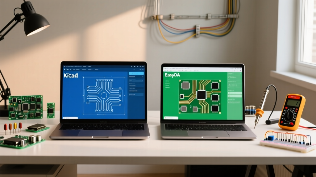

Selecting the right PCB drawing software dictates your entire workflow, from initial schematic capture to final Gerber export. While enterprise electronic design automation (EDA) tools cost thousands of dollars annually, the open-source and freemium maker ecosystem has matured to the point where you can route complex, multi-layer impedance-controlled boards without spending a dime on licensing. The challenge is no longer finding a tool; it is choosing the one that aligns with your specific fabrication pipeline and offline requirements.
The PCB Drawing Software Decision Matrix
The EDA landscape for hobbyists and independent engineers largely boils down to two dominant platforms: KiCad and EasyEDA. Both are exceptionally capable, but they solve fundamentally different workflow problems. Use the decision path below to lock in your software choice.
| Criteria | KiCad 8.0+ | EasyEDA Pro |
|---|---|---|
| Execution Environment | Local / Offline (Windows, Mac, Linux) | Cloud-based or Local Client |
| Library Management | Local symbol/footprint libraries (full version control) | Cloud LCSC/JLCPCB integrated libraries |
| 3D STEP Export | Native, highly customizable | Available, but less flexible for MCAD integration |
| Fabrication Integration | Manual Gerber/BOM generation and upload | 1-click ordering to JLCPCB with real-time pricing |
The Decision Path
- IF you require strict offline capability, Git-based version control for your schematic files, and native 3D STEP export for mechanical enclosures → Pick KiCad.
- IF you prioritize rapid prototyping, cloud collaboration with remote team members, and seamless 1-click PCBA ordering from JLCPCB → Pick EasyEDA Pro.
- IF you are routing >8 layer HDI boards with blind/buried vias and have a corporate budget → Look at Altium Designer (outside standard maker scope).
Breadboard-to-PCB Migration: Mistakes That Survive the Jump
A working breadboard circuit is a proof of concept, not a finalized design. Breadboards hide electrical sins. The parasitic capacitance between adjacent rows (typically 2pF to 5pF) and the high inductance of long jumper wires can accidentally stabilize oscillators or mask power rail noise. When you transition to a PCB drawing software and lay out copper traces, those parasitics vanish, and dormant flaws become catastrophic failures.
Which Mistakes Survive the Migration?
The most common errors that survive the jump from breadboard to PCB involve power delivery and logic thresholds. On a breadboard, the long, messy power rails act as accidental low-pass filters. On a PCB, a tight, low-inductance power plane will ring violently if decoupling is inadequate. Furthermore, floating CMOS inputs that happened to sit at a stable logic high due to ambient breadboard leakage will float into the linear region on a clean PCB, causing massive current draw and thermal runaway.
The Migration Checklist
Before finalizing your schematic in your PCB drawing software, run this mandatory checklist:
- Decoupling Capacitors: Add a 100nF (0.1µF) X7R ceramic capacitor physically adjacent to every single VCC pin on every IC. Add bulk 10µF to 47µF capacitors at the main power entry points.
- Explicit Pull-ups/Pull-downs: Replace any reliance on breadboard leakage or internal microcontroller weak pull-ups on critical reset or enable lines with explicit external 10kΩ resistors.
- Pinout Verification: Verify every pinout against the manufacturer's silicon datasheet, not the breadboard wiring diagram or third-party tutorial. Pin 1 orientations vary wildly between component families.
- Ground Return Paths: Ensure analog ground returns are routed separately from noisy digital switching grounds, joining only at a single star-ground point or under the ADC of your microcontroller.
Sizing Traces: Copper Weight vs. Current Capacity
Once your schematic is clean, the physical layout begins. The most frequent question during routing is: what trace width does this current need? The answer relies on the IPC-2152 standard, which calculates trace width based on copper weight (thickness), allowable temperature rise, and whether the trace is on an outer or inner layer. Outer layers dissipate heat into the ambient air, while inner layers are entombed in FR4 fiberglass, which acts as a thermal insulator.
For a standard 2A continuous load on an outer layer with a conservative 10°C temperature rise, you need a 35 mil (0.89 mm) trace for 1oz copper, or a 20 mil (0.51 mm) trace for 2oz copper. Always use the Saturn PCB Toolkit for precise calculations, as older IPC-2221 nomographs are overly conservative for outer layers but dangerously optimistic for inner layers.
| Current (Amps) | 1oz Copper (Outer) - 10°C Rise | 2oz Copper (Outer) - 10°C Rise | 1oz Copper (Inner) - 10°C Rise |
|---|---|---|---|
| 0.5 A | 12 mil (0.30 mm) | 8 mil (0.20 mm) | 25 mil (0.64 mm) |
| 1.0 A | 20 mil (0.51 mm) | 12 mil (0.30 mm) | 45 mil (1.14 mm) |
| 2.0 A | 35 mil (0.89 mm) | 20 mil (0.51 mm) | 85 mil (2.16 mm) |
| 3.0 A | 50 mil (1.27 mm) | 30 mil (0.76 mm) | 130 mil (3.30 mm) |
| 5.0 A | 85 mil (2.16 mm) | 50 mil (1.27 mm) | 220 mil (5.59 mm) |
Assembly, Safety, and First-Spin Board Testing
When your fabricated boards arrive, the transition from digital PCB drawing software to physical assembly begins. Proper soldering technique and a methodical power-up sequence are critical to preventing instant destruction of your new hardware.
Soldering Alloys and Thermal Profiles
Your iron temperature must match your solder alloy. Using Sn63Pb37 (63/37 leaded eutectic) requires a tip temperature of 320°C to 340°C. This alloy melts at 183°C and wets exceptionally well. If you are mandated to use SAC305 (lead-free), you must increase your tip temperature to 350°C to 370°C to overcome its higher 217°C melting point and poorer wetting characteristics. Never exceed 380°C, or you will rapidly oxidize the iron tip and degrade the flux core.
First-Spin Board Testing Sequence
Never plug a newly assembled board directly into a wall adapter or an unrestricted USB port. Follow this numbered sequence to verify the hardware:
- Visual and Tactile Inspection: Examine the board under a magnifying lamp. Look for solder bridges between adjacent IC pins, cold joints, and missed components. Clean flux residue with 99% isopropyl alcohol and a stiff brush to prevent parasitic leakage currents.
- Short Circuit Verification: Set your multimeter to continuity or resistance mode. Probe the main VCC and GND test points. You should read a high resistance (typically >1kΩ) that slowly climbs as input capacitors charge. If you read < 5Ω, you have a solder bridge or a backwards polarized capacitor. Do not apply power.
- Current-Limited Power Up: Connect a benchtop power supply set to your nominal voltage (e.g., 5.0V). Crucially, set the Over Current Protection (OCP) limit to 100mA (or the expected idle draw of your specific circuit). Power the board.
- Thermal and Voltage Checks: If the supply does not trip into constant-current (CC) mode, immediately touch the microcontroller and voltage regulators. They should be room temperature. Probe the 3.3V and 1.8V rails with your multimeter to verify the LDOs are regulating correctly.
- Signal Validation: Connect your oscilloscope or logic analyzer to the primary communication buses (I2C, SPI, or UART) and verify the idle states and clock frequencies before connecting any external peripherals.
By strictly adhering to this testing protocol, you isolate faults to specific subsystems, ensuring that a simple routing error in your PCB drawing software doesn't result in a catastrophic component failure on your workbench.


